 Group
Group

JEE Semiconductor Electronics PYQs
JEE Semiconductor electronics PYQs form a significant section of JEE physics syllabus. They assist you in determining the type of questions that are posed in this chapter and the familiarity with the key concepts, semiconductors, intrinsic and extrinsic semiconductors, p-n junctions, diodes, rectifiers, transistors, logic gates, and digital electronics.
Questions in semiconductor electronics are normally in the form of direct numerical problems or simple concept questions in the exam. The good news is that when your fundamentals are clear then this chapter becomes very easy. After studying the concepts and having the necessary knowledge of what formula or idea to apply, it becomes much easier to answer questions. This chapter does not have to be considered very difficult. A source of one of the more scoring portions of JEE Physics with regular revision and smart practice, it can become.
Here, you will get to find a basic formula PDF, a list of essential JEE Semiconductor Electronics PYQs in the download format, some practice questions with answers and some additional questions that you need to solve independently. You will also get to know the general ones that students make and some simple tips that can be used to save time during the exam.
JEE Semiconductor Electronics Important PYQs PDF
This PDF can include the most important previous year questions from semiconductor electronics. It may cover topics like intrinsic and extrinsic semiconductors, p-type and n-type semiconductors, p-n junction diode, forward bias, reverse bias, rectifiers, transistor action, transistor as an amplifier, logic gates, and truth tables.
Practicing these questions will help you understand the exam pattern better. It will also improve your speed, accuracy, and confidence before the exam.
Important Formulas for JEE Semiconductor Electronics PYQs
You only need a few important formulas and ideas to solve most semiconductor electronics questions in JEE. These formulas help you understand current relations, transistor behaviour, logic gate output, and diode-based circuits more clearly.
You can download the full formula PDF from the link above. Here is a quick look at some of the main formulas:
Concept | Formula |
Current Relation in Transistor | Iₑ = Iᵦ + I𝒸 |
Current Gain in Common Base | α = I𝒸 / Iₑ |
Current Gain in Common Emitter | β = I𝒸 / Iᵦ |
Relation Between α and β | β = α / (1 − α) |
Relation Between β and α | α = β / (1 + β) |
Power | P = VI |
Ohm’s Law | V = IR |
Output of NOT Gate | Y = Ā |
Output of AND Gate | Y = A · B |
Output of OR Gate | Y = A + B |
Output of NAND Gate | Y = (A · B)̅ |
Output of NOR Gate | Y = (A + B)̅ |
These formulas are commonly used in questions based on transistors, current gain, p-n junction behaviour, and digital logic circuits. If you revise them properly, many JEE questions start to feel much easier.
Top 5 Common Mistakes to Avoid in JEE Semiconductor Electronics PYQs
Many students find semiconductor electronics confusing at first because it includes both electronic devices and logic-based concepts. But most mistakes happen because small details are missed while solving. Here are some common mistakes you should avoid:
Confusing p-type and n-type semiconductors
In p-type semiconductors, holes are the majority charge carriers, while in n-type semiconductors, electrons are the majority charge carriers. Many students mix this up in theory questions.
Forgetting the difference between forward bias and reverse bias
A diode behaves differently in forward bias and reverse bias. If you do not remember this clearly, questions based on p-n junctions can become confusing.
Mixing up transistor current relations
Students often forget the relation between emitter current, base current, and collector current. A small mistake in current relation can change the final answer.
Making mistakes in logic gate outputs
AND, OR, NAND, NOR, and NOT gates may look simple, but students often confuse their truth tables and outputs.
Not reading the circuit carefully
In electronic circuit questions, a small detail in the diagram matters a lot. If you do not identify the device or connection correctly, the whole answer can go wrong.
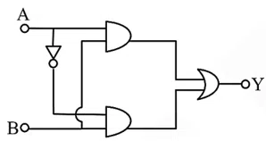
List of JEE Semiconductor Electronics PYQs
Here is a short set of JEE-style semiconductor electronics questions for practice. These include common question types from semiconductors, diodes, transistors, and logic gates. Solving them regularly can help you become faster and more confident.
Question 1
The charge stored by the capacitor C in the given circuit in the steady state is ______ $$\mu C$$.
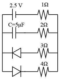
correct answer:- 3
Question 2
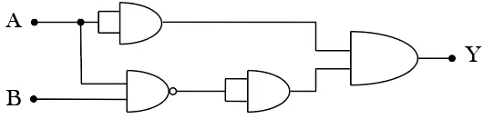
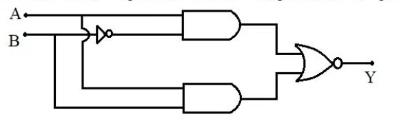
The given circuit works as:
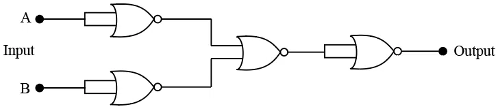
correct answer:- 3
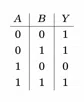
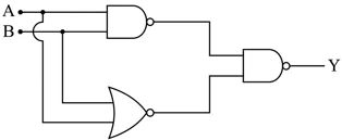
Question 3
The correct truth table for the given input data of the following logic gate is:
correct answer:- 4
Question 4
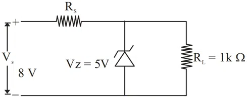
The following diagram shows a Zener diode as a voltage regulator. The Zener diode is rated at $$V_{z}=5V$$ and the desired current in load is 5 mA. The unregulated voltage source can supply upto 25 V. Considering the Zener diode can withstand four times of the load current, the value of resistor $$R_{s}$$ (shown in circuit) should be ____ Ω .
correct answer:- 4
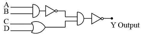
Question 5
Find the correct combination of A, B, C and D inputs which can cause the LED to glow.
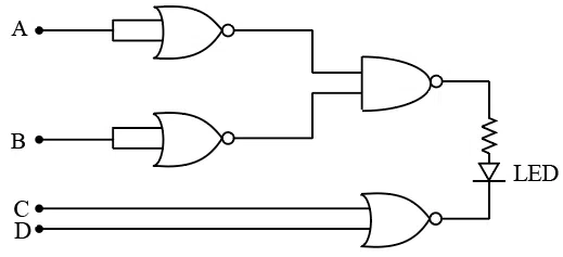
correct answer:- 4

Question 6
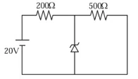
A voltage regulating circuit consisting of Zener diode, having break-down voltage of 10 V and maximum power dissipation of 0.4 W, is operated at 15 V. The approximate value of protective resistance in this circuit is ___ Ω.
correct answer:- 125
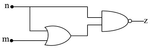
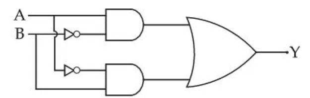
Question 7
Identify the correct truth table of the given logic circuit.
correct answer:- 2
Question 8
Assuming in forward bias condition there is a voltage drop of 0.7V across a silicon diode, the current through diode $$D_{1}$$ in the circuit is ___ mA.
(Assume all diodes in the given circuit are identical)
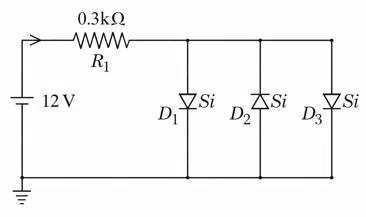
correct answer:- 1
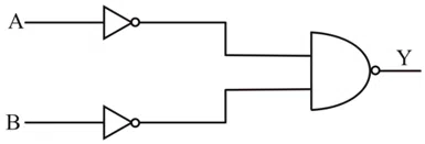
Question 9
For the given logic gate circuit, which of the following is the correct truth table?
correct answer:- 4
Question 10
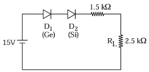
Two p-n junction diodes $$D_{1}\text{ and }D_{2}$$ are connected as shown in figure. A and B are input signals and C is the output. The given circuit will function as a________.
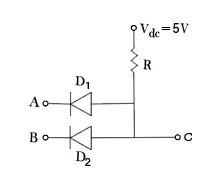
correct answer:- 3

Question 11
To obtain the given truth table, following logic gate should be placed at G:
correct answer:- 3
Question 12
Which of the following circuits represents a forward biased diode?
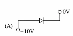
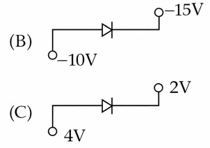
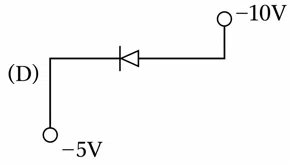
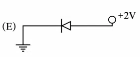
Choose the correct answer from the options given below :
correct answer:- 4
Question 13
Consider the following statements: A. The junction area of solar cell is made very narrow compared to a photo diode. B. Solar cells are not connected with any external bias. C. LED is made of lightly doped p-n junction. D. Increase of forward current results in continuous increase of LED light intensity. E. LEDs have to be connected in forward bias for emission of light. Choose the correct answer from the options given below:
correct answer:- 1
Question 14
The output of the circuit is low (zero) for:
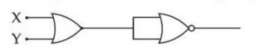
$$(A)\; X=0,\,Y=0 \text{ }(B)\; X=0,\,Y=1 \text{ }(C)\; X=1,\,Y=0 \text{ }(D)\; X=1,\,Y=1$$ Choose the correct answer from the options given below:
correct answer:- 1
Question 15
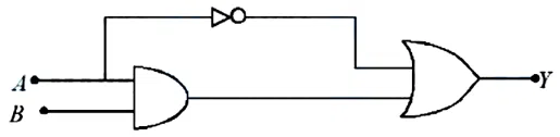
Which of the following circuits has the same outpur as that of the given circuit?
correct answer:- 2

Question 16
For the circuit shown above, equivalent GATE is :
correct answer:- 1
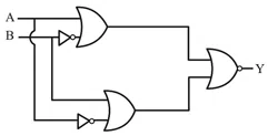
Question 17
The truth table for the circuit given below is :
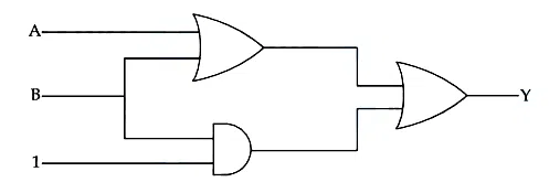
correct answer:- 4
Question 18
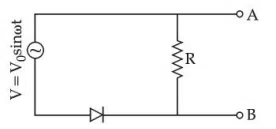
In the circuit shown here, assuming threshold voltage of diode is negligibly small, then voltage $$V_{AB}$$ is correctly represented by :
correct answer:- 4
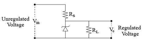
Question 19
In the given circuit if the power rating of Zener diode is $$10$$ mW, the value of series resistance $$R_s$$ to regulate the input unregulated supply is:
correct answer:- 1
Question 20
Conductivity of a photodiode starts changing only if the wavelength of incident light is less than 660 nm. The band gap of photodiode is found to be $$\frac{X}{8}$$ eV. The value of X is: (Given $$h = 6.6 \times 10^{-34}$$ J s, $$e = 1.6 \times 10^{-19}$$ C)
correct answer:- 1

Question 21
Which of the following circuits is reverse-biased?
correct answer:- 4
Question 22
The truth table of the given circuit diagram is :
correct answer:- 4
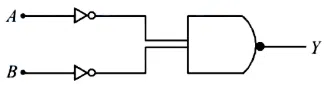
Question 23
The truth table for this given circuit is:
correct answer:- 2
Question 24
A Zener diode of breakdown voltage $$10 \text{ V}$$ is used as a voltage regulator as shown in the figure. The current through the Zener diode is
correct answer:- 3
Question 25
In the given circuit, the voltage across load resistance $$(R_L)$$ is:
correct answer:- 1

Question 26
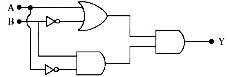
Identify the logic operation performed by the given circuit.
correct answer:- 3
Question 27
The output of the given circuit diagram is
correct answer:- 3
Question 28
Identify the logic gate given in the circuit:
correct answer:- 4
Question 29
Which of the diode circuit shows correct biasing used for the measurement of dynamic resistance of p-n junction diode:
correct answer:- 3
Question 30
The output $$(Y)$$ of logic circuit given below is 0 only when
correct answer:- 3
Question 31
Following gates section is connected in a complete suitable circuit.
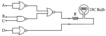
For which of the following combination, bulb will glow (ON) :
correct answer:- 3
Question 32
Given below are two statements: Statement I : Bromination of phenol in solvent with low polarity such as $$CHCl_3$$ or $$CS_2$$ requires Lewis acid catalyst. Statement II : The Lewis acid catalyst polarises the bromine to generate $$Br^+$$. In the light of the above statements, choose the correct answer from the options given below :
correct answer:- 3
Question 33
The correct truth table for the following logic circuit is :
correct answer:- 1
Question 34
Given below are two statements : Statement I : Picric acid is 2,4,6 - trinitrotoluene. Statement II : Phenol - 2,4 - disulphonic acid is treated with Conc. $$HNO_3$$ to get picric acid. In the light of the above statements, choose the most appropriate answer from the options given below :
correct answer:- 1
Question 35
In Reimer - Tiemann reaction, phenol is converted into salicylaldehyde through an intermediate. The structure of intermediate is _____
correct answer:- 1
Question 36
The acceptor level of a p-type semiconductor is $$6 \text{ eV}$$. The maximum wavelength of light which can create a hole would be : Given $$hc = 1242 \text{ eVnm}$$.
correct answer:- 3
Question 37
Match List - I with List - II.
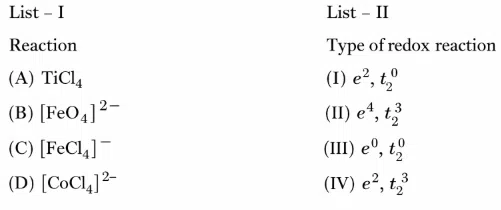
Choose the correct answer from the options given below :
correct answer:- 3
Question 38
The output Y of following circuit for given inputs is :
correct answer:- 2
Question 39
Identify the major products A and B respectively in the following set of reactions.
correct answer:- 4
Question 40
Which one of the following compounds will readily react with dilute NaOH?
correct answer:- 2
.webp)


