

 Group
Group
 Group
Group


 Preferred Source

 Google Discover

JEE Electronic Devices PYQs
JEE Electronic Devices PYQs are an important part of the JEE Physics syllabus. Practising these questions helps you understand key topics such as semiconductors, p-n junctions, diodes, rectifiers, transistors, logic gates, and basic digital circuits.
Questions from Electronic Devices may appear in JEE as direct concept-based questions, simple numericals, or circuit-based problems. This chapter can feel different from other Physics chapters because it focuses more on how electronic components work. Once you understand the basic behaviour of each device, the questions become much easier to solve.
Instead of trying to memorise every circuit or result, focus on understanding the working principle behind each component. Regular revision and practice with JEE Electronic Devices Questions can improve your conceptual clarity and help you solve questions faster. Solving chapter-wise JEE Questions, attempting a JEE Mains Mock Test, and practising from a JEE Mains Previous Papers can also help you understand the actual exam pattern.
In this blog, you will find an Electronic Devices Formula Sheet, important JEE Electronic Devices PYQs in downloadable format, practice questions with answers, and a few extra problems for self-practice. You will also learn about common mistakes students make in this chapter and simple ways to avoid them during the exam.
JEE Electronic Devices Important PYQs PDF
This PDF can include some of the most useful previous-year questions from Electronic Devices. The questions may cover intrinsic and extrinsic semiconductors, p-n junction diodes, Zener diodes, rectifiers, transistors, logic gates, Boolean expressions, and digital electronics.
Practising these questions will help you understand the type of problems commonly asked in JEE. It can also improve your accuracy, confidence, and ability to read electronic circuits correctly. Solving questions from a JEE Mains Previous Paper is especially useful because it gives you a better idea of the level and style of the actual exam.
Important Electronic Devices Formula Sheet for JEE
You only need a few important formulas and logic rules to solve most questions from this chapter. These are mainly used in problems related to diodes, transistors, rectifiers, current gain, power, and digital logic.
| Concept | Formula |
|---|---|
| Ohm’s Law | $$V = IR$$ |
| Current Gain in CE Mode | $$\beta = \frac{I_C}{I_B}$$ |
| Current Gain in CB Mode | $$\alpha = \frac{I_C}{I_E}$$ |
| Relation Between α and β | $$\beta = \frac{\alpha}{1-\alpha}$$ |
| Diode Current Equation | $$I = I_0\left(e^{\frac{eV}{kT}}-1\right)$$ |
| AND Gate Output | $$Y = A\cdot B$$ |
| OR Gate Output | $$Y = A+B$$ |
| NOT Gate Output | $$Y = \overline{A}$$ |
| Electrical Power | $$P = VI$$ |
| Rectifier Efficiency | $$\eta = \frac{P_{\mathrm{dc}}}{P_{\mathrm{ac}}}$$ |
These formulas and expressions are commonly used in questions based on semiconductor devices, diodes, transistors, rectifiers, and logic gates. Revising them along with reliable JEE Study Material can help you remember the important relationships and avoid small mistakes.
Top 5 Common Mistakes to Avoid in JEE Electronic Devices PYQs
Many students lose marks in this chapter because of small conceptual errors rather than difficult calculations. Here are some common mistakes you should watch out for:
Confusing intrinsic and extrinsic semiconductors
Intrinsic semiconductors are pure, while extrinsic semiconductors are formed by adding impurities. Make sure you understand the difference between n-type and p-type materials as well.
Using the wrong diode bias
Always check whether the diode is forward biased or reverse biased before deciding how current will flow through the circuit.
Mixing up transistor currents
Emitter, base, and collector currents are related, but they are not equal. Remember the basic relation Iₑ = I꜀ + Iᵦ before solving transistor questions.
Forgetting logic-gate outputs
Students often confuse AND, OR, NAND, NOR, XOR, and NOT gates. Revising their truth tables regularly can help you avoid easy mistakes.
Ignoring the circuit diagram
Many questions in this chapter are based on small circuit diagrams. Read the connections carefully before applying any formula or rule.
Regular practice with chapter-wise questions and a JEE Mains Mock Test can help you identify these mistakes early and improve your accuracy.
List of JEE Electronic Devices PYQs
Below is a test-style set of questions based on semiconductors, diodes, transistors, rectifiers, logic gates, and digital electronics. Try to solve each question on your own before checking the answer.
Question 1
An n-type semiconductor sample is prepared by doping pure Silicon with a pentavalent impurity. At a temperature of $$300 \,\, \text{K}$$, the intrinsic carrier concentration of Silicon is $$n_i = 1.5 \times 10^{16} \,\, \text{m}^{-3}$$. If the donor impurity concentration added to the crystal is $$N_D = 4.5 \times 10^{22} \,\, \text{m}^{-3}$$, the concentration of holes ($$p_n$$) in this doped semiconductor sample at the same temperature is:
correct answer:- 1
Question 2
The height of a transmitting antenna at the top of a tower is $$25$$ m and that of receiving antenna is, $$49$$ m. The maximum distance between them, for satisfactory communication in LOS (Line-Of-Sight) is $$K\sqrt{5} \times 10^2$$ m. The value of $$K$$ is ______.
(Assume radius of Earth is $$64 \times 10^5$$ m) [Calculate upto nearest integer value]
correct answer:- 192
Question 3
For a transistor in CE mode to be used as an amplifier, it must be operated in:
correct answer:- 3
Question 4
The temperature dependence of resistance of Cu and undoped Si in the temperature range 300 - 400 K is best described by:
correct answer:- 1
Question 5
In a common emitter amplifier circuit using an $$n$$-$$p$$-$$n$$ transistor, the phase difference between the input and the output voltages will be:
correct answer:- 1

Question 6
In a semiconductor p-n diode, the doping concentrations on p-side has $$10^{15}$$ atoms/cm³ and the n-side has $$10^{18}$$ atoms/cm³respectively. Which one of the following statements is true?
correct answer:- 2
Question 7
Which of the following modulated signal has the best noise-tolerance?
correct answer:- 2
Question 8
The photodiode is used to detect the optical signals. These diodes are preferably operated in reverse biased mode because
correct answer:- 4
Question 9
A system of four gates is set up as shown. The 'truth table' corresponding to this system is :
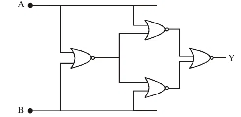
correct answer:- 1
Question 10
Which of the following circuits represents a forward biased diode?
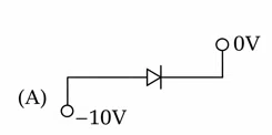
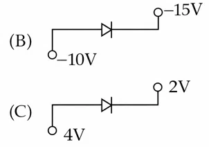
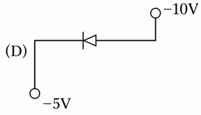
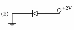
Choose the correct answer from the options given below :
correct answer:- 4

Question 11
Match List I with List II
| List I | List II |
|---|---|
| (A) Facsimile | (I) Static Document Image |
| (B) Guided media Channel | (II) Local Broadcast Radio |
| (C) Frequency Modulation | (III) Rectangular wave |
| (D) Digital Signal | (IV) Optical Fiber |
correct answer:- 2
Question 12
The output of the circuit is low (zero) for:

$$(A)\; X=0,\,Y=0 \text{ }(B)\; X=0,\,Y=1 \text{ }(C)\; X=1,\,Y=0 \text{ }(D)\; X=1,\,Y=1$$ Choose the correct answer from the options given below:
correct answer:- 1
Question 13
The energy band gap of semiconducting material to produce violet (wavelength $$= 4000$$ $$\mathring{A}$$) LED is ______ eV. (Round off to the nearest integer).
correct answer:- 3
Question 14
In the figure, given that $$V_{BB}$$ supply can vary from 0 to 5.0 V, $$V_{CC} = 5$$ V, $$\beta_{dc} = 200$$, $$R_B = 100$$ k$$\Omega$$, $$R_C = 1$$ k$$\Omega$$ and $$V_{BE} = 1.0$$ V. The minimum base current and the input voltage at which the transistor will go to saturation, will be, respectively:
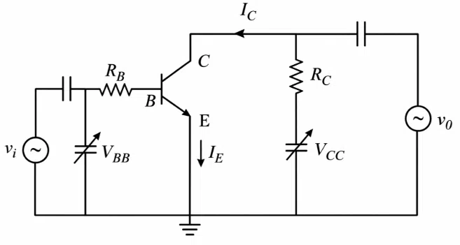
correct answer:- 3
Question 15
An NPN transistor operates as a common emitter amplifier, with a power gain of 60 dB. The input circuit resistance is 100 Ω and the output load resistance is 10 kΩ. The common emitter current gain β is:
correct answer:- 2

Question 16
The transfer characteristic curve of a transistor, having input and output resistance 100 Ω and 100 kΩ respectively, is shown in the figure. The voltage and power gain, are respectively:
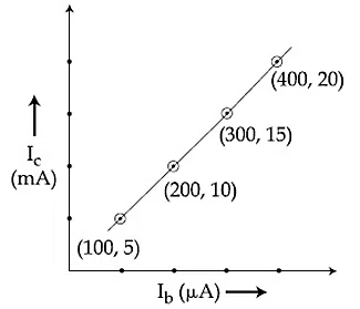
correct answer:- 1
Question 17
Identify the correct output signal $$Y$$ in the given combination of gates (as shown $$n$$) for the given inputs $$A$$ and $$B$$:
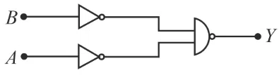
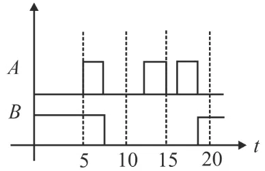
correct answer:- 3
Question 18
Two Zener diodes ($$A$$ and $$B$$) having breakdown voltages of $$6\,\text{V}$$ and $$4\,\text{V}$$ respectively, are connected as shown in the circuit below. The output voltage $$V_0$$ variation with input voltage linearly increasing with time, is given by ($$V_{input} = 0V$$ at $$t = 0$$):
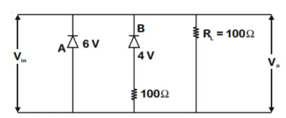
correct answer:- 3
Question 19
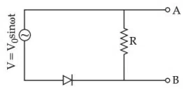
In the circuit shown here, assuming threshold voltage of diode is negligibly small, then voltage $$V_{AB}$$ is correctly represented by :
correct answer:- 4
Question 20
In a Zener regulated power supply, a Zener diode with a breakdown voltage of $$V_Z = 6 \,\, \text{V}$$ is connected in series with a protective resistance $$R_S = 100 \,\, \Omega$$ across an unregulated DC source of $$10 \,\, \text{V}$$. If a load resistance of $$R_L = 300 \,\, \Omega$$ is connected in parallel with the Zener diode, the current flowing through the Zener diode ($$I_Z$$) is:
correct answer:- 2

Question 21
Consider the following two statements regarding an unbiased $$p\text{-}n$$ junction diode at room temperature:
Statement I: The diffusion current across the junction flows from the $$p\text{-type}$$ region to the $$n\text{-type}$$ region because of the concentration gradient of charge carriers.
Statement II: The drift current flows in the opposite direction (from $$n\text{-type}$$ to $$p\text{-type}$$) due to the internal electric field set up in the depletion layer.
In the light of the above statements, choose the correct answer from the options given below:
correct answer:- 2
Question 22
In a pure (intrinsic) semiconductor, the concentration of charge carriers is $$n_i = 1.5 \times 10^{16} \text{ m}^{-3}$$ at room temperature. It is doped with a pentavalent impurity such that the electron concentration increases to $$n_e = 4.5 \times 10^{22} \text{ m}^{-3}$$. The concentration of holes ($$n_h$$) in this extrinsic semiconductor is:
correct answer:- 1
Question 23
In the digital circuit shown in the figure, for the given inputs the P and Q values are :
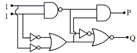
correct answer:- 2
Question 24
The output $$Y$$ for the inputs $$A$$ and $$B$$ of circuit is given by
Truth table of the shown circuit is:
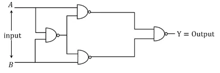
correct answer:- 4
Question 25
In the following circuit, the reading of the ammeter will be (Take Zener breakdown voltage = 4 V)
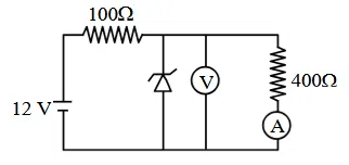
correct answer:- 3

Question 26
In an experiment of CE configuration of $$n-p-n$$ transistor, the transfer characteristics are observed as given in figure. If the input resistance is $$200\Omega$$ and output resistance is $$60\Omega$$, the voltage gain in this experiment will be ______.
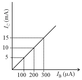
correct answer:- 15
Question 27
Identify the correct Logic Gate for the following output ($$Y$$) of two inputs $$A$$ and $$B$$.
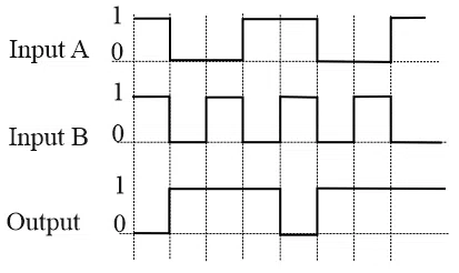
correct answer:- 2
Question 28
Match List-I with List-II
| List-I | List-II |
|---|---|
| (A) Television signal | (I) 03 KHz |
| (B) Radio signal | (II) 20 KHz |
| (C) High Quality Music | (III) 02 MHz |
| (D) Human speech | (IV) 06 MHz |
correct answer:- 3
Question 29
In the given circuit, the value of current $$I_L$$ will be ______ mA. (When $$R_L = 1$$ k$$\Omega$$)
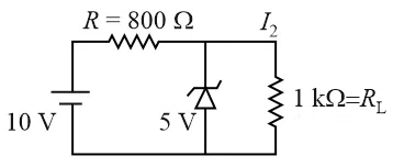
correct answer:- 5
Question 30
Two 4 bits binary numbers, $$A = 1101$$ and $$B = 1010$$ are given in the inputs of a logic circuit shown in figure below . The output $$(Y)$$ will be :
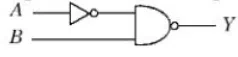
correct answer:- 1
Question 31
A signal of $$100$$ THz frequency can be transmitted with maximum efficiency by
correct answer:- 2
.webp)