Two p-n junction diodes $$D_{1}\text{ and }D_{2}$$ are connected as shown in figure. A and B are input signals and C is the output. The given circuit will function as a________.
Sign in
Please select an account to continue using cracku.in
↓ →
Join Our JEE Preparation Group
Prep with like-minded aspirants; Get access to free daily tests and study material.
Two p-n junction diodes $$D_{1}\text{ and }D_{2}$$ are connected as shown in figure. A and B are input signals and C is the output. The given circuit will function as a________.
Let 0V represent Logic 0 and
5V represent Logic 1.
Case 1: If either input A or B (or both) is at 0V (Logic 0), the respective diode is forward-biased. This pulls the output voltage at node C down to 0V.
Result: If A = 0 or B = 0, then output C = 0.
Case 2: If both inputs A and B are at 5V (Logic 1), both diodes $$D_1$$ and $$D_2$$ are reverse-biased and act as open circuits. Since no current flows through resistor R, the output C remains pulled up to 5V.
Result: If A = 1 and B = 1, then output C = 1.
Truth Table:
The above truth table corresponds exactly to an AND gate.
The following diagram shows a Zener diode as a voltage regulator. The Zener diode is rated at $$V_{z}=5V$$ and the desired current in load is 5 mA. The unregulated voltage source can supply upto 25 V. Considering the Zener diode can withstand four times of the load current, the value of resistor $$R_{s}$$ (shown in circuit) should be ____ Ω .
Identify the correct truth table of the given logic circuit.
If X and Y are the inputs, the given circuit works as :
Assume positive-logic levels: LOW = $$0\text{ V}$$, HIGH = $$+5\text{ V}$$. In the given network the anodes of two identical silicon diodes are tied to the input lines $$X$$ and $$Y$$, while their cathodes meet at node $$O$$. Node $$O$$ is pulled up to $$+5\text{ V}$$ through a resistor $$R_L$$ (the load resistor) and is the output.
Step 1 - Input combination $$X = 0$$, $$Y = 0$$
Both anodes are at $$0\text{ V}$$. Each diode is forward-biased (anode $$0\text{ V}$$, cathode initially $$5\text{ V}$$). They conduct and clamp node $$O$$ close to $$0.7\text{ V}$$ (the diode drop). The output is interpreted as LOW.
Step 2 - Input combination $$X = 0$$, $$Y = 1$$
The diode connected to $$X$$ is forward-biased (anode $$0\text{ V}$$), so it again pulls node $$O$$ to about $$0.7\text{ V}$$. The other diode is reverse-biased, but the conducting one is enough to keep the output LOW.
Step 3 - Input combination $$X = 1$$, $$Y = 0$$
This is symmetrical to Step 2. The diode linked with $$Y$$ conducts, forcing the output LOW (≈$$0.7\text{ V}$$).
Step 4 - Input combination $$X = 1$$, $$Y = 1$$
Now both diode anodes and cathodes sit at $$+5\text{ V}$$, so each diode is reverse-biased. No current flows through the diodes. The pull-up resistor $$R_L$$ therefore lifts node $$O$$ to $$+5\text{ V}$$, producing a HIGH output.
Step 5 - Truth table
$$\begin{array}{ccc|c} X & Y & & O \\ \hline 0 & 0 & & 0 \\ 0 & 1 & & 0 \\ 1 & 0 & & 0 \\ 1 & 1 & & 1 \\ \end{array}$$
This truth table is identical to that of a two-input AND gate.
Hence the circuit functions as an AND gate.
Option B which is: AND gate
The charge stored by the capacitor C in the given circuit in the steady state is ______ $$\mu C$$.
In second branch capacitor acts as an open circuit when in steady state.
The upper diode (in the 3 Ω branch) points left. Its cathode is at a higher
potential than its anode, meaning it is reverse-biased and acts as an
open circuit
The lower diode (in the 4 Ω branch) points right. Its anode is at a higher
potential, meaning it is forward-biased and acts as a short circuit (assuming an ideal diode)
$$R_{\text{eq}} = 1\,\Omega + 4\,\Omega = 5\,\Omega$$
$$I = \frac{V}{R_{\text{eq}}} = \frac{2.5}{5} = 0.5\text{ A}$$
The voltage across the capacitor, $$V_{C}$$ , is exactly equal to the potential difference between the left and
right common nodes.
$$V_C = I \times 4\,\Omega$$
$$V_C = 0.5 \times 4 = 2\text{ V}$$
$$Q = C \times V_C$$
$$Q = 5\,\mu\text{F} \times 2\text{ V}$$
$$Q = 10\,\mu\text{C}$$
The given circuit works as:
Middle Gate: NOR gate evaluating $$\overline{\overline{A} + \overline{B}}$$. By De Morgan's Law, this equals $$A \cdot B$$ (AND logic).
Find the correct combination of A, B, C and D inputs which can cause the LED to glow.

by checking for each option we obtain option D is correct
For the given circuit (shown in part (A)) the time dependent input voltage $$v_{in}(t)$$ and corresponding output $$v_o(t)$$ are shown in part (B) and part (C), respectively. Identify the components that are used in the circuit between points X and Y.
The input waveform shown in part (B) is an undistorted sinusoid that swings symmetrically above and below the 0-V axis.
The output waveform shown in part (C) is identical to the positive half-cycles of the input, whereas the entire negative half-cycles are missing (the output remains at 0 V whenever the input is negative).
This behaviour is the signature of an ideal half-wave rectifier:
• During the positive half-cycle, the rectifying element is forward-biased, it conducts, and $$v_{o}(t) \approx v_{in}(t)$$ (neglecting the small forward drop).
• During the negative half-cycle, the rectifying element is reverse-biased, it blocks, and the load sees no current, so $$v_{o}(t)=0$$.
The simplest circuit that realises a half-wave rectifier between the points X (input node) and Y (output node) is a single p-n diode (anode at X, cathode at Y) feeding a load resistor connected from Y to ground. No other passive component can reproduce exactly this “positive-half-only” transfer characteristic.
Hence the network between X and Y must consist of a forward-biased diode in series with the load, i.e. the arrangement given in Option A.
Option A which is: a single diode (anode at X, cathode at Y) forming a half-wave rectifier.
Two 4 bits binary numbers, $$A = 1101$$ and $$B = 1010$$ are given in the inputs of a logic circuit shown in figure below . The output $$(Y)$$ will be :
A pair of cross-connected NAND gates (as drawn in the question) behaves exactly like a 2-input Exclusive-OR (XOR) gate. For two logic levels $$a$$ and $$b$$ the circuit gives the function
$$Y = a \oplus b = \bar a\,b + a\,\bar b$$
Because the same arrangement is repeated for every corresponding bit, the 4-bit output $$Y_3Y_2Y_1Y_0$$ is obtained by XOR-ing each bit of $$A$$ with the same-position bit of $$B$$.
Write the two numbers from the most-significant bit (MSB) to the least-significant bit (LSB):
$$A = A_3A_2A_1A_0 = 1\;1\;0\;1$$
$$B = B_3B_2B_1B_0 = 1\;0\;1\;0$$
Now evaluate the XOR bit by bit using the rule $$1\oplus1=0,\;1\oplus0=1,\;0\oplus1=1,\;0\oplus0=0$$.
Bit-wise computation
MSB $$Y_3 = 1 \oplus 1 = 0$$
Next $$Y_2 = 1 \oplus 0 = 1$$
Next $$Y_1 = 0 \oplus 1 = 1$$
LSB $$Y_0 = 1 \oplus 0 = 1$$
Collecting the four results gives
$$Y = Y_3Y_2Y_1Y_0 = 0\;1\;1\;1 = 0111$$
Hence the output of the circuit is
Option C which is: $$Y = 0111$$
The correct truth table for the given input data of the following logic gate is:
Trick: To solve such questions in less time, it is advised to directly try options and eliminate them.

option D satisfies for all
The maximum rated power of the LED is 2 mW and it is used in the circuit with input voltage of 5 V as shown in the figure below. The current through resistance $$R_S$$ is 0.5 mA.
The minimum value of the resistance of $$R_S$$, to ensure that the LED is not damaged is _______ k$$\Omega$$.
Assuming in forward bias condition there is a voltage drop of 0.7V across a silicon diode, the current through diode $$D_{1}$$ in the circuit is ___ mA.
(Assume all diodes in the given circuit are identical)
Diodes D1 and D3 are forward-biased (ON).
Diode D2 is reverse-biased (OFF) and acts as an open circuit. Because $$D_1$$ and $$D_3$$ are in parallel, the voltage drop across this entire parallel combination is $$0.7\text{ V}$$.
The voltage across the resistor $$R_1$$
$$ V_{R1} = 12\text{ V} - 0.7\text{ V} = 11.3\text{ V} $$
$$ I_{\text{total}} = \frac{V_{R1}}{R_1} = \frac{11.3\text{ V}}{0.3\text{ k}\Omega} $$
$$ I_{\text{total}} = \frac{11.3}{0.3}\text{ mA} = \frac{113}{3}\text{ mA} $$
$$D_1$$ and $$D_3$$ are indentical and in parallel, the total current splits equally between them.
$$ I_{D1} = \frac{I_{\text{total}}}{2} $$
$$ I_{D1} = \frac{113/3\text{ mA}}{2} = \frac{113}{6}\text{ mA} $$
$$ I_{D1} \approx 18.83\text{ mA} $$
For the given logic gate circuit, which of the following is the correct truth table?
Consider a circuit consisting of a capacitor (20 $$\mu$$F), resistor (100 $$\Omega$$) and two identical diodes as shown in figure. The resistance of diode under forward biasing condition is 10 $$\Omega$$. The time constant of the circuit is $$\alpha \times 10^{-3}$$ s. The value of $$\alpha$$ is :
The time constant of an $$RC$$ network is given by
$$\tau = R_{\text{eq}}\,C$$
where
• $$C$$ is the capacitance, and
• $$R_{\text{eq}}$$ is the net resistance actually present in the current path that charges / discharges the capacitor.
Data from the problem:
• Capacitor: $$C = 20 \,\mu\text{F} = 20 \times 10^{-6}\,\text{F}$$
• Fixed resistor: $$R = 100\,\Omega$$
• Two identical diodes whose forward (dynamic) resistance is $$r_d = 10\,\Omega$$ each.
Because the two diodes are connected with opposite orientation (as is usual in such clipping / rectifying circuits), only one diode is forward-biased at any instant. Hence, along the conduction path there is:
$$R_{\text{eq}} = R + r_d = 100\,\Omega + 10\,\Omega = 110\,\Omega$$
Therefore, the time constant becomes
$$\tau = R_{\text{eq}}\,C = 110\,\Omega \times 20 \times 10^{-6}\,\text{F}$$
$$\tau = 2200 \times 10^{-6}\,\text{s} = 2.2 \times 10^{-3}\,\text{s}$$
Comparing with $$\tau = \alpha \times 10^{-3}\,\text{s}$$, we get
$$\alpha = 2.2$$
Hence, the correct choice is
Option A which is: $$2.2$$
Refer to the logic circuit given below. For two inputs $$(A = 1, B = 1)$$ and $$(A = 0, B = 1)$$, output (Y) will be __________.
For the given logic circuit, which of the following inputs combination will make both LED-1 and LED-2 to glow?
Let’s decode the circuit step-by-step.
step 1: identify gates
• first gate (A, B) → OR gate
→ output = A + B
This output goes to:
• LED-1
• one input of next gate
step 2: second gate
inputs:
• (A + B)
• C
this is an AND gate
so output = (A + B) · C
step 3: final gate
inputs:
• A (direct wire from top)
• (A + B)C
this is AND
so final output:
= A · (A + B) · C
but:
A · (A + B) = A
so:
final output = A · C
step 4: LED conditions
LED-1 glows when:
A + B = 1
LED-2 glows when:
A · C = 1
step 5: combine conditions
for both LEDs ON:
A · C = 1 ⇒ A = 1, C = 1
then A + B = 1 is already satisfied (since A = 1)
so B can be 0 or 1
final answer:
(A, B, C) = (1, 0, 1) or (1, 1, 1)
Given below are two statements: one is labelled as Assertion A and the other is labelled as Reason R
Assertion A: A diode under reverse-biased condition provides very small current which is nearly independent of voltage until a critical limit at which the current increases drastically.
Reason R: Below the critical voltage limit, only majority charge carriers flow which increases drastically above critical voltage.
Choose the correct answer from the options given below :
In a $$p$$-$$n$$ junction diode the biasing conditions decide the direction and magnitude of current.
Let the applied voltage be $$V$$ with the convention that forward bias is positive and reverse bias is negative.
Behaviour under reverse bias
• When the junction is reverse-biased, the depletion region widens and the majority carriers are repelled away from the junction.
• The only carriers that are able to cross the junction are the thermally generated minority carriers (electrons in the $$p$$-region and holes in the $$n$$-region).
• Their concentration is fixed by temperature, not by the magnitude of the reverse voltage (as long as the electric field is below the breakdown limit).
• Hence the reverse current remains almost constant and is called the reverse saturation current $$I_S$$.
When the reverse voltage magnitude becomes large enough, the electric field in the depletion region exceeds a critical value. Avalanche multiplication (or Zener tunnelling, depending on doping) starts, causing a sudden, very large increase in reverse current. This point is called the breakdown voltage $$V_{BR}$$.
Verification of Assertion (A)
The statement in (A) says: “A reverse-biased diode gives a small current independent of voltage until a critical limit is reached.”
This is exactly the description of the constant reverse saturation current up to the breakdown voltage. Therefore Assertion (A) is true.
Verification of Reason (R)
Reason (R) states: “Below the critical voltage, only majority carriers flow.”
This is incorrect because, under reverse bias, majority carriers are blocked by the widened potential barrier. The small reverse current is due to minority carriers, not majority carriers. Hence the Reason (R) is false.
Relationship between A and R
Since (A) is true and (R) is false, (R) cannot be the correct explanation of (A).
Therefore, the correct choice is:
Option C which is: A is true but R is false.
In a semiconductor p-n diode, the doping concentrations on p-side has $$10^{15}$$ atoms/cm³ and the n-side has $$10^{18}$$ atoms/cm³respectively. Which one of the following statements is true?
The output $$Y$$ for the given inputs $$A$$ and $$B$$ to the circuit is :
A diode has Zener voltage of 10 V and maximum power dissipation of 0.5 W, then the minimum resistance to be used in series with this diode for safety when it is connected to a 25 V power supply is ______ $$\Omega$$.
The Zener diode will operate in its breakdown (regulating) region when the voltage across it is $$V_Z = 10\text{ V}$$.
Its maximum power dissipation is $$P_{\text{max}} = 0.5\text{ W}$$.
Using the power formula $$P = VI$$, the maximum permissible current through the Zener is
$$I_{\text{Z(max)}} = \frac{P_{\text{max}}}{V_Z} = \frac{0.5\text{ W}}{10\text{ V}} = 0.05\text{ A} = 50\text{ mA}.$$
The supply voltage is $$V_S = 25\text{ V}$$. A series resistor $$R_S$$ is placed so that, at the worst case (no external load, all current through the Zener), the current does not exceed $$I_{\text{Z(max)}}$$.
Applying Kirchhoff’s Voltage Law:
$$V_S = I_{\text{Z}}\,R_S + V_Z.$$
At the limiting condition, $$I_{\text{Z}} = I_{\text{Z(max)}}$$. Hence
$$R_S = \frac{V_S - V_Z}{I_{\text{Z(max)}}} = \frac{25\text{ V} - 10\text{ V}}{0.05\text{ A}} = \frac{15\text{ V}}{0.05\text{ A}} = 300\ \Omega.$$
Therefore, the minimum series resistance required is 300 Ω.
A voltage regulating circuit consisting of Zener diode, having break-down voltage of 10 V and maximum power dissipation of 0.4 W, is operated at 15 V. The approximate value of protective resistance in this circuit is ___ Ω.
We need to find the protective resistance in a Zener diode voltage regulating circuit.
Zener breakdown voltage: $$V_Z = 10$$ V
Maximum power dissipation of Zener: $$P_{max} = 0.4$$ W
Supply voltage: $$V_S = 15$$ V
$$I_Z = \frac{P_{max}}{V_Z} = \frac{0.4}{10} = 0.04 \text{ A} = 40 \text{ mA}$$
The voltage drop across the protective resistance:
$$V_R = V_S - V_Z = 15 - 10 = 5 \text{ V}$$
The protective resistance must limit the current through the Zener to its maximum value (assuming no load current, worst case):
$$R = \frac{V_R}{I_Z} = \frac{5}{0.04} = 125 \, \Omega$$
Therefore, the approximate value of the protective resistance is 125 ohm.
To obtain the given truth table, following logic gate should be placed at G:
The output after each AND gate is $$ A \cdot \overline{B} $$ which means the same input to G.
By putting values of $$ A $$ and $$ B $$ from the truth table and by eliminating options, we get G to be a NOR gate.
Consider the following statements: A. The junction area of solar cell is made very narrow compared to a photo diode. B. Solar cells are not connected with any external bias. C. LED is made of lightly doped p-n junction. D. Increase of forward current results in continuous increase of LED light intensity. E. LEDs have to be connected in forward bias for emission of light. Choose the correct answer from the options given below:
Let us analyze each statement:
A. The junction area of solar cell is made very narrow compared to a photodiode.
This is false. In a solar cell, the junction area is made very large (not narrow) to capture maximum sunlight. It is the photodiode that typically has a smaller junction area.
B. Solar cells are not connected with any external bias.
This is true. Solar cells operate on the photovoltaic effect and generate their own EMF. They work without any external bias — they are essentially self-biased by the sunlight.
C. LED is made of lightly doped p-n junction.
This is false. LEDs are made of heavily doped p-n junctions to ensure high recombination rates and efficient light emission.
D. Increase of forward current results in continuous increase of LED light intensity.
This is false. Initially, increasing forward current increases light intensity, but beyond a certain point, the LED may reach saturation or get damaged. The increase is not continuous — there is a maximum rated current.
E. LEDs have to be connected in forward bias for emission of light.
This is true. LEDs emit light when electrons and holes recombine at the junction, which occurs only under forward bias.
The correct statements are B and E only.
The answer is Option A: B, E Only.
Choose the correct logic circuit for the given truth table having inputs A and B.
The output of the circuit is low (zero) for:
$$(A)\; X=0,\,Y=0 \text{ }(B)\; X=0,\,Y=1 \text{ }(C)\; X=1,\,Y=0 \text{ }(D)\; X=1,\,Y=1$$ Choose the correct answer from the options given below:
The truth table for the circuit given below is :
The output voltage in the following circuit is (Consider ideal diode case) :
Which of the following circuits represents a forward biased diode?
Choose the correct answer from the options given below :
A p-n junction diode is forward biased when the electric potential at its p-side (anode, represented by the triangle) is strictly greater than the electric potential at its n-side (cathode, represented by the straight line). The condition for forward bias is $$V_p > V_n$$.
Option A: The p-side is connected to $$-10 \text{ V}$$ and the n-side is connected to $$0 \text{ V}$$. Since $$-10 \text{ V} < 0 \text{ V}$$, meaning $$V_p < V_n$$, this diode is reverse biased.
Option B: The p-side is connected to $$-10 \text{ V}$$ and the n-side is connected to $$-15 \text{ V}$$. Since $$-10 \text{ V} > -15 \text{ V}$$, meaning $$V_p > V_n$$, this diode is forward biased.
Option C: The p-side is connected to $$4 \text{ V}$$ and the n-side is connected to $$2 \text{ V}$$. Since $$4 \text{ V} > 2 \text{ V}$$, meaning $$V_p > V_n$$, this diode is also forward biased.
Option D: The n-side is connected to $$-5 \text{ V}$$ and the p-side is connected to $$-10 \text{ V}$$. Since $$-5 \text{ V} > -10 \text{ V}$$, meaning $$V_n> V_p$$, this diode is also reverse biased.
Option E: The n-side is connected to ground, which is $$0 \text{ V}$$, and the p-side is connected to $$+2 \text{ V}$$. Since $$0 \text{ V} < +2 \text{ V}$$, meaning $$V_n < V_p$$, this diode is forward biased.
Based on the explicit values shown in the provided circuit diagrams, circuits B, C, and E all represent forward biased diodes
Consider the following logic circuit. The output is Y = 0 when :
A zener diode with 5V zener voltage is used to regulate an unregulated dc voltage input of 25 V. For a 400 $$\Omega$$ resistor connected in series, the zener current is found to be 4 times load current. The load current ($$I_L$$) and load resistance ($$R_L$$) are:
The zener diode keeps the voltage across itself and the parallel load fixed at $$V_Z = 5\text{ V}$$.
The source voltage is $$V_S = 25\text{ V}$$ and the series resistor is $$R_S = 400\,\Omega$$.
Hence the voltage across $$R_S$$ equals $$V_S - V_Z = 25 - 5 = 20\text{ V}$$.
Current through the series resistor (which is the sum of zener current $$I_Z$$ and load current $$I_L$$) is therefore
$$I_S = \frac{20}{400} = 0.05\text{ A} = 50\text{ mA}$$ $$-(1)$$
Given that the zener current is four times the load current,
$$I_Z = 4 I_L$$ $$-(2)$$
From $$I_S = I_Z + I_L$$ and substituting from $$(2)$$:
$$I_S = 4 I_L + I_L = 5 I_L$$ $$-(3)$$
Using $$(1)$$ and $$(3)$$:
$$5 I_L = 50\text{ mA} \;\Longrightarrow\; I_L = 10\text{ mA}$$
The load resistance is found from Ohm’s law using the regulated voltage:
$$R_L = \frac{V_Z}{I_L} = \frac{5\text{ V}}{10\text{ mA}} = 500\,\Omega$$
Thus, $$I_L = 10\text{ mA}$$ and $$R_L = 500\,\Omega$$. This matches Option D.
For the circuit shown above, equivalent GATE is :
In the digital circuit shown in the figure, for the given inputs the P and Q values are :
The truth table corresponding to the circuit given below is
The Boolean expression $$Y = \overline{A}BC + \overline{A}C$$ can be realised with which of the following gate configurations.
A. One 3-input AND gate, 3 NOT gates and one 2-input OR gate, One 2-input AND gate,
B. One 3-input AND gate, 1 NOT gate, One 2-input NOR gate and one 2-input OR gate
C. 3-input OR gate, 3 NOT gates and one 2-input AND gate
Choose the correct answer:
Consider a n-type semiconductor in which $$n_e$$ and $$n_h$$ are number of electrons and holes, respectively.
(A) Holes are minority carriers
(B) The dopant is a pentavalent atom
(C) $$n_e n_h \neq n_i^2$$
(where $$n_{i}$$ is number of electrons or holes in semiconductor when it is intrinsic form)
(D) $$n_e n_h \geq n_i^2$$
(E) The holes are not generated due to the donors
Choose the correct answer from the options given below :
In an extrinsic semiconductor, one type of charge carrier is made the majority by adding a suitable impurity. If the dopant supplies extra electrons, the material becomes n-type.
Step 1 : Nature of majority and minority carriers
In an n-type semiconductor, electrons supplied by donor atoms are the majority carriers, while holes created by thermal generation are very few in number.
Thus statement (A) “Holes are minority carriers” is TRUE.
Step 2 : Kind of dopant required
A silicon or germanium atom has four valence electrons. To donate an extra electron we must insert an element from group V (P, As, Sb, etc.) which has five valence electrons. Such an atom is called a pentavalent donor.
Therefore statement (B) “The dopant is a pentavalent atom” is TRUE.
Step 3 : Applying the mass-action law
At thermal equilibrium, semiconductors (intrinsic or extrinsic) obey the mass-action law
$$n_e n_h = n_i^2 \quad -(1)$$
where $$n_i$$ is the intrinsic carrier concentration.
Hence the product $$n_e n_h$$ always equals, not differs from, $$n_i^2$$.
• Statement (C) “$$n_e n_h \neq n_i^2$$” contradicts equation $$(1)$$, so it is FALSE.
• Statement (D) “$$n_e n_h \geq n_i^2$$” is also inconsistent with $$(1)$$ (equality must hold), so it is FALSE.
Step 4 : Origin of the minority holes
In an n-type material, donor atoms produce extra electrons only. Holes arise solely from the thermal breaking of covalent bonds (electron-hole pair generation), exactly as in an intrinsic semiconductor. They are not created by the donor atoms.
Therefore statement (E) “The holes are not generated due to the donors” is TRUE.
Step 5 : Collecting the TRUE statements
TRUE : (A), (B), (E)
FALSE : (C), (D)
Comparing with the given options, Option C lists exactly (A), (B), (E).
Hence the correct answer is Option C.
Which of the following circuits has the same output as that of the given circuit?

In the circuit shown here, assuming threshold voltage of diode is negligibly small, then voltage $$V_{AB}$$ is correctly represented by :
A light emitting diode (LED) is fabricated using GaAs semiconducting material whose band gap is $$1.42$$ eV. The wavelength of light emitted from the LED is :
For an LED, the wavelength of emitted light is related to the band gap by:
$$E = \frac{hc}{\lambda}$$
Rearranging for $$\lambda$$ gives:
$$\lambda = \frac{hc}{E}$$ = $$\frac{1240 \text{ eV·nm}}{E \text{ (eV)}}$$
With $$E = 1.42$$ eV, we have
$$\lambda = \frac{1240}{1.42} \approx 873.2 \text{ nm} \approx 875 \text{ nm}$$
Therefore, the correct answer is Option 3: 875 nm.
Identify the logic gate given in the circuit:
$$A$$ after NOT gate is $$ \overline{A} $$.
$$B$$ after NOT gate is $$ \overline{B} $$.
$$ \overline{A} $$ and $$ \overline{B} $$ are inputs to the NAND gate.
$$ Y = \overline{ \overline{A} \cdot \overline{B} } $$
Using De Morgan's law:
$$ Y = A + B $$
i.e., it is an OR gate.
In the given circuit if the power rating of Zener diode is $$10$$ mW, the value of series resistance $$R_s$$ to regulate the input unregulated supply is:
In the given circuit, the voltage across load resistance $$(R_L)$$ is:
The acceptor level of a p-type semiconductor is $$6 \text{ eV}$$. The maximum wavelength of light which can create a hole would be : Given $$hc = 1242 \text{ eVnm}$$.
To create a hole in a p-type semiconductor, an electron must be excited from the valence band to the acceptor energy level. The minimum energy required for this transition is the energy gap of the acceptor level.
$$ E = 6 \text{ eV} $$
$$ E = \frac{hc}{\lambda} $$
$$ \lambda_{max} = \frac{hc}{E} $$
$$ hc = 1242 \text{ eVnm} $$
$$ E = 6 \text{ eV} $$
$$ \lambda_{max} = \frac{1242}{6} $$
$$ \lambda_{max} = 207 \text{ nm} $$
The correct truth table for the following logic circuit is :
The $$I - V$$ characteristics of an electronic device shown in the figure. The device is:
The output of the given circuit diagram is
output of this upper OR gate be $$Y_1$$:
$$ Y_1 = A + \overline{B} $$
the output of this lower gate be $$Y_2$$:
$$ Y_2 = \overline{A} + B $$
The final logic gate is a NOR gate
$$ Y = \overline{Y_1 + Y_2} $$
$$ Y = \overline{(A + \overline{B}) + (\overline{A} + B)} $$
$$ Y = \overline{(A + \overline{A}) + (B + \overline{B})} $$
According to Boolean algebra rules, the OR operation between a variable and its complement is always 1
($$A + \overline{A} = 1$$ and $$B + \overline{B} = 1$$):
$$ Y = \overline{1 + 1} $$
$$ Y = \overline{1} $$
$$ Y = 0 $$
The output Y of following circuit for given inputs is :
The output $$(Y)$$ of logic circuit given below is 0 only when
output of the top OR gate is A+B
output of the bottom AND gate is B(since B.1=B)
now these two are the inputs fed to final OR gate whose output is A+B+B
which is equal to A+B
Now A+B is 0 only when both A=0 and B=0
The truth table of the given circuit diagram is :
Which of the following circuits is reverse-biased?
A Zener diode of breakdown voltage $$10 \text{ V}$$ is used as a voltage regulator as shown in the figure. The current through the Zener diode is
Conductivity of a photodiode starts changing only if the wavelength of incident light is less than 660 nm. The band gap of photodiode is found to be $$\frac{X}{8}$$ eV. The value of X is: (Given $$h = 6.6 \times 10^{-34}$$ J s, $$e = 1.6 \times 10^{-19}$$ C)
The conductivity of the photodiode changes when the wavelength of incident light is less than or equal to 660 nm. This wavelength corresponds to the minimum photon energy required to excite electrons across the band gap, which equals the band gap energy $$E_g$$.
The energy of a photon is given by:
$$E = \frac{hc}{\lambda}$$
where:
Substitute the values:
$$E = \frac{(6.6 \times 10^{-34}) \times (3 \times 10^8)}{6.6 \times 10^{-7}}$$
Simplify the expression:
Numerator: $$6.6 \times 10^{-34} \times 3 \times 10^8 = 19.8 \times 10^{-26} = 1.98 \times 10^{-25}$$
Denominator: $$6.6 \times 10^{-7}$$
So,
$$E = \frac{1.98 \times 10^{-25}}{6.6 \times 10^{-7}} = \frac{1.98}{6.6} \times 10^{-25 + 7} = 0.3 \times 10^{-18} = 3 \times 10^{-19} \, \text{J}$$
This energy is in joules, but the band gap is given in electron volts (eV). The conversion factor is $$1 \, \text{eV} = 1.6 \times 10^{-19} \, \text{J}$$. Therefore, convert energy to eV:
$$E_g = \frac{3 \times 10^{-19}}{1.6 \times 10^{-19}} = \frac{3}{1.6} = 1.875 \, \text{eV}$$
The problem states that the band gap is $$\frac{X}{8} \, \text{eV}$$. So,
$$\frac{X}{8} = 1.875$$
Solving for $$X$$:
$$X = 1.875 \times 8 = 15$$
Thus, the value of $$X$$ is 15.
Following gates section is connected in a complete suitable circuit.
For which of the following combination, bulb will glow (ON) :
Identify the logic operation performed by the given circuit.

In the truth table of the above circuit the value of $$X$$ and $$Y$$ are :
The truth table for this given circuit is:
Which of the diode circuit shows correct biasing used for the measurement of dynamic resistance of p-n junction diode:
Match List - I with List - II.

Choose the correct answer from the options given below :
Given below are two statements : Statement I : Picric acid is 2,4,6 - trinitrotoluene. Statement II : Phenol - 2,4 - disulphonic acid is treated with Conc. $$HNO_3$$ to get picric acid. In the light of the above statements, choose the most appropriate answer from the options given below :
Statement I: Picric acid is 2,4,6-trinitrophenol (NOT trinitrotoluene — that's TNT). Statement I is incorrect.
Statement II: Phenol-2,4-disulphonic acid treated with conc. HNO₃ gives picric acid (the sulphonic acid groups are replaced by nitro groups). Statement II is correct.
The correct answer is Option (1): Statement I is incorrect but Statement II is correct.
Given below are two statements: Statement I : Bromination of phenol in solvent with low polarity such as $$CHCl_3$$ or $$CS_2$$ requires Lewis acid catalyst. Statement II : The Lewis acid catalyst polarises the bromine to generate $$Br^+$$. In the light of the above statements, choose the correct answer from the options given below :
Statement I: Bromination of phenol in solvent with low polarity ($$CHCl_3$$ or $$CS_2$$) requires Lewis acid catalyst.
Phenol is a highly activated aromatic ring (due to the $$-OH$$ group donating electron density). Even in low polarity solvents, phenol does NOT require a Lewis acid catalyst for bromination — it reacts directly with $$Br_2$$ to give mono-brominated product (p-bromophenol as the major product). The Lewis acid catalyst is needed for benzene, not phenol. Statement I is false.
Statement II: The Lewis acid catalyst polarises bromine to generate $$Br^+$$.
This is the correct mechanism of Lewis acid catalysed bromination. The Lewis acid (like $$FeBr_3$$ or $$AlBr_3$$) complexes with $$Br_2$$ to generate a highly electrophilic $$Br^+$$ (or its equivalent). Statement II is true.
The correct answer is Option (3): Statement I is false but Statement II is true.
Identify the major products A and B respectively in the following set of reactions.
In Reimer - Tiemann reaction, phenol is converted into salicylaldehyde through an intermediate. The structure of intermediate is _____
Which one of the following compounds will readily react with dilute NaOH?
Since NaOH is a base, we need to find which compound is sufficiently acidic to react with dilute NaOH.
Ethanol ($$C_2H_5OH$$) is an aliphatic alcohol with very weak acidity (pKa ~ 16), so it does not react with dilute NaOH.
Phenol ($$C_6H_5OH$$) is a weak acid (pKa ~ 10) due to resonance stabilization of the phenoxide ion; it readily reacts with NaOH:
$$C_6H_5OH + NaOH \rightarrow C_6H_5ONa + H_2O$$
Benzyl alcohol ($$C_6H_5CH_2OH$$) is a primary alcohol and not acidic enough to react with dilute NaOH, and tert-butanol ($$(CH_3)_3COH$$) is a tertiary alcohol that likewise does not react with dilute NaOH.
Therefore, among the given compounds only phenol ($$C_6H_5OH$$) is acidic enough to react with dilute NaOH. The correct answer is Option 2: $$C_6H_5OH$$.
In the following sequence of reaction, the major products B and C respectively are :
For the given logic gates combination, the correct truth table will be
If each diode has a forward bias resistance of 25$$\Omega$$ in the below circuit, which of the following options is correct?
Name the logic gate equivalent to the diagram attached
Which of the following statement is not correct in the case of light emitting diodes?
A. It is a heavily doped p-n junction.
B. It emits light only when it is forward biased.
C. It emits light only when it is reverse biased.
D. The energy of the light emitted is equal to or slightly less than the energy gap of the semiconductor used.
Choose the correct answer from the options given below:
We analyze each statement about Light Emitting Diodes (LEDs):
Statement A: "It is a heavily doped p-n junction." — This is correct. LEDs are made from heavily doped p-n junctions to ensure efficient radiative recombination of electrons and holes.
Statement B: "It emits light only when it is forward biased." — This is correct. Under forward bias, electrons and holes recombine at the junction, releasing energy as photons.
Statement C: "It emits light only when it is reverse biased." — This is incorrect. LEDs emit light under forward bias, not reverse bias. Under reverse bias, there is no significant recombination of charge carriers at the junction.
Statement D: "The energy of the light emitted is equal to or slightly less than the energy gap of the semiconductor used." — This is correct. The photon energy $$h\nu$$ is approximately equal to the band gap $$E_g$$, and can be slightly less due to thermal effects and other energy loss mechanisms.
The only incorrect statement is C.
The correct answer is Option C: C.
A zener diode of power rating 1.6 W is to be used as voltage regulator. If the zener diode has a breakdown of 8 V and it has to regulate voltage fluctuating between 3 V and 10 V. The value of resistance $$R_s$$ for safe operation of diode will be
Given: Power rating = 1.6 W, breakdown voltage $$V_z = 8$$ V, input voltage fluctuates between 3 V and 10 V.
Maximum zener current: $$I_{z,max} = \frac{P}{V_z} = \frac{1.6}{8} = 0.2$$ A
For safe operation, the maximum current through the zener should not exceed 0.2 A. This occurs when the input voltage is maximum (10 V).
The series resistance $$R_s$$ must limit the current:
$$R_s = \frac{V_{input,max} - V_z}{I_{z,max}} = \frac{10 - 8}{0.2} = \frac{2}{0.2} = 10 \text{ } \Omega$$
The correct answer is Option 1: 10 $$\Omega$$.
Choose the correct statement about Zener diode:
We need to identify the correct statement about a Zener diode.
Key properties of a Zener diode:
In forward bias, a Zener diode behaves just like a normal p-n junction diode. It conducts current once the forward voltage exceeds the typical threshold (~0.7 V for silicon).
In reverse bias, a Zener diode is specifically designed to undergo controlled breakdown at a well-defined voltage called the Zener breakdown voltage. Once this voltage is reached, the voltage across the diode remains nearly constant even as current varies. This property makes it function as a voltage regulator in reverse bias.
Evaluating the options:
Option A: "It works as a voltage regulator in reverse bias and behaves like simple p-n junction diode in forward bias." This is correct.
Option B: "It works as a voltage regulator in both forward and reverse bias." This is incorrect — in forward bias it does not regulate voltage.
Option C: "It works as a voltage regulator only in forward bias." This is incorrect — it regulates voltage in reverse bias, not forward bias.
Option D: "It works as a voltage regulator in forward bias and behaves like simple p-n junction diode in reverse bias." This is incorrect — it reverses the actual behavior.
The correct answer is Option A.
For a given transistor amplifier circuit in CE configuration $$V_{CC} = 1$$ V, $$R_C = 1$$ k$$\Omega$$, $$R_b = 100$$ k$$\Omega$$ and $$\beta = 100$$. Value of base current $$I_b$$ is
For the logic circuit shown, the output waveform at Y is
Given below are two statements: one is labelled as Assertion A and the other is labelled as Reason R
Assertion A: Photodiodes are used in forward bias usually for measuring the light intensity.
Reason R: For a $$p-n$$ junction diode, at applied voltage $$V$$ the current in the forward bias is more than the current in the reverse bias for $$|V_z| > \pm V \geq |V_0|$$ where $$V_0$$ is the threshold voltage and $$V_z$$ is the breakdown voltage.
In the light of the above statements, choose the correct answer from the options given below
We need to evaluate the Assertion-Reason statement about photodiodes.
Assertion A: Photodiodes are used in forward bias usually for measuring the light intensity.
Analysis of A: This is FALSE. Photodiodes are used in reverse bias (or zero bias/photovoltaic mode) for measuring light intensity. In reverse bias, the photocurrent is proportional to the light intensity, and the dark current is minimal, making it ideal for light detection.
Reason R: For a $$p$$-$$n$$ junction diode, at applied voltage $$V$$, the current in forward bias is more than the current in reverse bias for $$|V_z| > \pm V \geq |V_0|$$, where $$V_0$$ is the threshold voltage and $$V_z$$ is the breakdown voltage.
Analysis of R: This is TRUE. For a p-n junction diode, in the voltage range between the threshold voltage and the breakdown voltage, the forward bias current is indeed greater than the reverse bias current. In reverse bias, only a small saturation current flows (until breakdown), whereas in forward bias beyond $$V_0$$, current increases exponentially.
Conclusion: Assertion A is false, but Reason R is true.
The correct answer is Option C: A is false but R is true.
Given below are two statements: one is labelled as Assertion A and the other is labelled as Reason R
Assertion A: Diffusion current in a p-n junction is greater than the drift current in magnitude if the junction is forward biased.
Reason R: Diffusion current in a p-n junction is from the n-side to the p-side if the junction is forward biased.
At any p-n junction two carrier-transport mechanisms exist simultaneously:
• Diffusion current, produced by the gradient in majority-carrier concentration.
• Drift current, produced by the electric field inside the depletion region.
Under thermal equilibrium the two currents are equal and opposite, so the net current is zero:
$$J_{\text{diff}} + J_{\text{drift}} = 0$$ $$-(1)$$
Forward bias applied
• The external forward voltage $$V_F$$ lowers the junction (barrier) potential $$V_0 - V_F$$.
• A lower barrier allows many more majority carriers (electrons from the n-side and holes from the p-side) to cross the junction by diffusion.
• The diffusion current therefore increases exponentially with the applied forward voltage: $$J_{\text{diff}} \propto e^{\frac{qV_F}{kT}}$$.
• The drift current depends mainly on the magnitude of the electric field inside the depletion region. That field decreases only slightly when the diode is forward biased, so $$J_{\text{drift}}$$ changes very little.
Consequently, in forward bias
$$\left|J_{\text{diff}}\right| \gt\!\!\left|J_{\text{drift}}\right|$$ $$-(2)$$
Statement A is therefore correct.
Direction of the diffusion current in forward bias
• Electron concentration is high on the n-side and low on the p-side. Electrons diffuse from the n-side towards the p-side.
• Hole concentration is high on the p-side and low on the n-side. Holes diffuse from the p-side towards the n-side.
• For conventional current we add the two contributions. Electrons moving n→p represent conventional current in the same n→p direction (negative charge moving n→p is equivalent to positive current n→p with a minus sign, but the two carrier types together give a net diffusion current that we describe as flowing from the n-side to the p-side).
Hence, when the junction is forward biased, the diffusion current is considered to flow from the n-side to the p-side. This makes Assertion R correct.
Relation between R and A
The very fact that majority carriers diffuse from the side of higher concentration (n) to the side of lower concentration (p) explains why their diffusion component grows rapidly once the barrier is lowered, and therefore why it overtakes the drift component in magnitude. Thus R provides the physical reason for A.
Both Assertion A and Reason R are correct, and R is the correct explanation of A.
Hence, the correct option is Option D.
Given below are two statements: one is labelled as Assertion A and the other is labelled as Reason R.
Assertion A: Photodiodes are preferably operated in reverse bias condition for light intensity measurement.
Reason R: The current in the forward bias is more than the current in the reverse bias for a $$p - n$$ junction diode.
In the light of the above statement, choose the correct answer from the options given below :
Assertion A: Photodiodes are preferably operated in reverse bias condition for light intensity measurement.
Reason R: The current in forward bias is more than the current in reverse bias for a p-n junction diode.
Evaluation of Assertion A:
In reverse bias, a photodiode has a very small dark current. When light falls on it, the photogenerated carriers (electron-hole pairs) contribute to a current that is directly proportional to the light intensity. This makes the change in current due to light easily measurable. In forward bias, the large forward current would overwhelm the photocurrent, making measurement difficult. Assertion A is true.
Evaluation of Reason R:
In a p-n junction diode, forward bias current is indeed much larger than reverse bias current (reverse bias gives only a small leakage current). Reason R is true.
Does R explain A?
The reason photodiodes are used in reverse bias is specifically because the small reverse current makes it easier to detect light-induced changes. While R states a true fact about diode currents, it does not directly explain why reverse bias is preferred for light measurement (it does not mention photocurrent sensitivity or signal-to-noise ratio). So R is not the correct explanation of A.
Both A and R are true but R is NOT the correct explanation of A. The answer is Option 2.
In an n-p-n common emitter (CE) transistor the collector current changes from $$5$$ mA to $$16$$ mA for the change in base current from $$100 \ \mu$$A and $$200 \ \mu$$A, respectively. The current gain of transistor is _____.
Match the List I with List II
A. Intrinsic Semiconductor I. Fermi-level near valence band
B. n-type semiconductor II. Fermi-level at middle of valence and conduction band
C. p-type semiconductor III. Fermi-level near conduction band
D. Metals IV. Fermi-level inside conduction band
Let us match each type of material with the position of its Fermi level:
A. Intrinsic Semiconductor - In an intrinsic (pure) semiconductor, the number of electrons in the conduction band equals the number of holes in the valence band. The Fermi level lies at the middle of the valence and conduction band (II).
B. n-type Semiconductor - In an n-type semiconductor, donor impurities provide extra electrons. The Fermi level shifts upward, near the conduction band (III).
C. p-type Semiconductor - In a p-type semiconductor, acceptor impurities create extra holes. The Fermi level shifts downward, near the valence band (I).
D. Metals - In metals, free electrons are abundant and the Fermi level lies inside the conduction band (IV).
Therefore, the correct matching is: (A) $$\to$$ II, (B) $$\to$$ III, (C) $$\to$$ I, (D) $$\to$$ IV.
The effect of increase in temperature on the number of electrons in conduction band $$(n_e)$$ and resistance of a semiconductor will be as:
In a semiconductor, increasing the temperature has two effects:
1. Number of electrons in conduction band ($$n_e$$) increases:
Higher temperature provides more thermal energy to electrons in the valence band, allowing more of them to overcome the band gap and jump to the conduction band. This increases $$n_e$$.
2. Resistance decreases:
With more charge carriers (both electrons and holes) available for conduction, the conductivity of the semiconductor increases. Since resistance is inversely proportional to conductivity, the resistance decreases.
Therefore, $$n_e$$ increases and resistance decreases with increasing temperature.
The logic gate equivalent to the given circuit diagram is:
The logic operations performed by the given digital circuit is equivalent to:
Let the two external inputs be labelled as $$A$$ and $$B$$.
Step 1 - Identify each block in the diagram.
• Each small triangle with a bubble at its output is an INVERTER (NOT gate).
• The larger gate whose symbol has a curved input side and a bubble at its output is a NOR gate.
Step 2 - Write the Boolean expression of every stage.
• Output of the first inverter is $$\overline{A}$$.
• Output of the second inverter is $$\overline{B}$$.
• The NOR gate receives $$\overline{A}$$ and $$\overline{B}$$, so its output $$Y$$ is
$$Y = \overline{\overline{A} + \overline{B}} \quad -(1)$$
Step 3 - Simplify the expression using De Morgan’s theorem.
De Morgan’s theorem states
$$\overline{X + Z} = \overline{X} \cdot \overline{Z}$$
Applying this to $$(1)$$ with $$X = \overline{A}$$ and $$Z = \overline{B}$$ gives
$$Y = \overline{\overline{A}} \cdot \overline{\overline{B}}$$
Since a double negation cancels, $$\overline{\overline{A}} = A$$ and $$\overline{\overline{B}} = B$$. Hence
$$Y = A \cdot B$$
Step 4 - Interpret the final Boolean result.
The output expression $$Y = A \cdot B$$ is the logical AND of the inputs.
Therefore, the overall operation performed by the given circuit is an AND gate.
Option B (AND) is correct.
The logic performed by the circuit shown in figure is equivalent to
The output waveform of the given logical circuit for the following inputs $$A$$ and $$B$$ as shown below, is
The resistivity $$(\rho)$$ of semiconductor varies with temperature. Which of the following curve represents the correct behaviour?
A modulating signal is a square wave, as shown in the figure. If the carrier wave is given as $$c(t) = 2\sin(8\pi t)$$ volts, the modulation index is:
The given modulating signal is a square wave of amplitude
$$A_m = 1$$
Amplitude of carrier wave:
$$A_c = 2$$
Modulation index is given by
$$\mu = \frac{A_m}{A_c}$$
Substituting the values,
$$\mu = \frac{1}{2}$$
Hence,
$$\boxed{\mu=\frac{1}{2}}$$
Statement I: When a Si sample is doped with Boron, it becomes P type and when doped by Arsenic it becomes N-type semi conductor such that P-type has excess holes and N-type has excess electrons.
Statement II: When such P-type and N-type semi-conductors, are fused to make a junction, a current will automatically flow which can be detected with an externally connected ammeter.
In the light of above statements, choose the most appropriate answer from the options given below.
In the following circuit, the correct relation between output ($$Y$$) and inputs $$A$$ and $$B$$ will be
To determine the logic operation of the given circuit, we analyze the behavior of the diodes and the NPN transistor for different input combinations:
The first part of the circuit (diodes $$D_1$$ and $$D_2$$ connected to a $$-10\text{ V}$$ source through resistor R) acts as an AND gate logic for the point X:
The NPN transistor acts as a NOT gate (inverter):
| Input A | Input B | Point X (A ⋅ B) | Output Y (X) |
| 0 | 0 | 0 | 1 |
| 1 | 0 | 0 | 1 |
| 0 | 1 | 0 | 1 |
| 1 | 1 | 1 | 0 |
The output Y is the inverse of the AND operation of the inputs. This corresponds to a NAND gate.
Correct Relation:
$$\boxed{Y = \overline{AB}}$$
Correct Option: (C)
For using a multimeter to identify diode from electrical components, choose the correct statement out of the following about the diode
We need to identify the correct statement about a diode when using a multimeter.
Understanding a Diode:
A diode is a semiconductor device with two terminals — the anode and the cathode.
Key Property of a Diode:
A diode conducts current in only one direction (forward bias). In reverse bias, it blocks current (except for a negligible leakage current).
Using a Multimeter to Identify a Diode:
When we use a multimeter in diode-test mode:
- In one orientation (forward bias): the multimeter shows a low resistance/voltage drop, indicating current flows.
- In the reverse orientation (reverse bias): the multimeter shows very high resistance (open circuit), indicating no current flows.
Evaluating the Options:
Option A: "Conducts current in both directions" — This describes a resistor, not a diode. Incorrect.
Option B: "Two terminal device which conducts current in one direction only" — This is the correct description of a diode.
Option C: "Does not conduct current, gives an initial deflection which decays to zero" — This describes a capacitor. Incorrect.
Option D: "Three terminal device" — A diode has only two terminals, not three. This describes a transistor. Incorrect.
Hence, the correct answer is Option B.
A logic gate circuit has two inputs $$A$$ and $$B$$ and output $$Y$$. The voltage waveforms of $$A$$, $$B$$ and $$Y$$ are shown. The logic gate circuit is
We need to identify the logic gate from the voltage waveforms of inputs $$A$$, $$B$$ and output $$Y$$.
From the waveforms, let us construct the truth table by reading the HIGH (1) and LOW (0) values of $$A$$, $$B$$, and $$Y$$ at each time interval:
Interval 1: $$A = 0, B = 0 \Rightarrow Y = 0$$
Interval 2: $$A = 1, B = 0 \Rightarrow Y = 0$$
Interval 3: $$A = 1, B = 1 \Rightarrow Y = 1$$
Interval 4: $$A = 0, B = 1 \Rightarrow Y = 0$$
Now let us compare this with the truth tables of the given gates:
AND gate truth table:
$$A = 0, B = 0 \Rightarrow Y = 0$$
$$A = 1, B = 0 \Rightarrow Y = 0$$
$$A = 1, B = 1 \Rightarrow Y = 1$$
$$A = 0, B = 1 \Rightarrow Y = 0$$
The output $$Y$$ is HIGH only when both $$A$$ and $$B$$ are HIGH. This matches perfectly with the AND gate truth table.
The correct answer is Option A: AND gate.
An n.p.n transistor with current gain $$\beta = 100$$ in common emitter configuration is shown in figure. The output voltage of the amplifier will be
For a constant collector-emitter voltage of 8 V, the collector current of a transistor reached to the value of 6 mA from 4 mA, whereas base current changed from $$20 \ \mu A$$ to $$25 \ \mu A$$ value. If transistor is in active state, small signal current gain (current amplification factor) will be
We are given:
Collector-emitter voltage: $$V_{CE} = 8$$ V (constant)
Collector current changes from $$I_{C1} = 4$$ mA to $$I_{C2} = 6$$ mA
Base current changes from $$I_{B1} = 20\ \mu A$$ to $$I_{B2} = 25\ \mu A$$
Recall the formula for small signal current gain. The small signal current gain (AC current amplification factor) is defined as:
$$\beta_{ac} = \frac{\Delta I_C}{\Delta I_B}\bigg|_{V_{CE} = \text{constant}}$$
Calculate the changes in currents. $$\Delta I_C = I_{C2} - I_{C1} = 6 - 4 = 2 \text{ mA} = 2 \times 10^{-3} \text{ A}$$ and $$\Delta I_B = I_{B2} - I_{B1} = 25 - 20 = 5\ \mu A = 5 \times 10^{-6} \text{ A}$$
Calculate the small signal current gain: $$\beta_{ac} = \frac{2 \times 10^{-3}}{5 \times 10^{-6}} = \frac{2000}{5} = 400$$
The correct answer is Option B: 400.
For a transistor to act as a switch, it must be operated in
We need to determine in which region a transistor must operate to act as a switch.
Understanding transistor as a switch:
A switch has two states — ON and OFF.
OFF state (Cut-off region): When no base current flows (or the base-emitter voltage is below the threshold), both junctions are reverse biased. No collector current flows, and the transistor acts like an open switch.
ON state (Saturation region): When sufficient base current flows, both junctions are forward biased. Maximum collector current flows, and the transistor acts like a closed switch with very low resistance.
The active region is used for amplification, not switching, because in this region the collector current is proportional to the base current (linear behaviour).
Therefore, for a transistor to act as a switch, it must operate in the saturation and cut-off regions — switching between these two states.
The correct answer is Option B.
Given below are two statements : One is labelled as Assertion A and the other is labelled as Reason R.
Assertion A : $$n - p - n$$ transistor permits more current than a $$p - n - p$$ transistor.
Reason R : Electrons have greater mobility as a charge carrier.
We need to evaluate both the Assertion and the Reason about transistors.
Assertion A: An $$n-p-n$$ transistor permits more current than a $$p-n-p$$ transistor.
Analysis of Assertion A:
In an $$n-p-n$$ transistor, the majority charge carriers are electrons, while in a $$p-n-p$$ transistor, the majority charge carriers are holes.
Since the mobility of electrons is greater than the mobility of holes, the $$n-p-n$$ transistor allows more current to flow for the same applied voltage.
Therefore, Assertion A is true.
Reason R: Electrons have greater mobility as a charge carrier.
Analysis of Reason R:
This is a well-known fact. In semiconductors, the mobility of electrons ($$\mu_e$$) is greater than the mobility of holes ($$\mu_h$$).
Therefore, Reason R is true.
Is R the correct explanation of A?
Yes. The reason the $$n-p-n$$ transistor permits more current is precisely because electrons (the charge carriers in $$n-p-n$$) have higher mobility than holes (the charge carriers in $$p-n-p$$). So Reason R directly explains Assertion A.
Hence, the correct answer is Option A: Both A and R are true, and R is the correct explanation of A.
Identify the logic operation performed by the given circuit
Identify the solar cell characteristics from the following options:
In the given circuit the input voltage $$V_{in}$$ is shown in figure. The cut-in voltage of $$p-n$$ junction diode ($$D_1$$ or $$D_2$$) is 0.6 V. Which of the following output voltage ($$V_0$$) waveform across the diode is correct?
The photodiode is used to detect the optical signals. These diodes are preferably operated in reverse biased mode because
A photodiode is used to detect optical signals and is preferably operated in reverse bias mode.
Why reverse bias?
In reverse bias, the current through the photodiode is primarily due to minority carriers. When light falls on the junction, it generates electron-hole pairs (minority carriers in their respective regions).
In reverse bias mode, the dark current (without light) is very small since it depends only on minority carriers. When light is incident, the photogenerated minority carriers cause a significant fractional change in the total current.
This fractional change in minority carriers produces a higher reverse bias current, making the photodiode more sensitive to optical signals in reverse bias mode.
In forward bias, the current is dominated by majority carriers, and the small photocurrent due to minority carriers would be negligible compared to the large forward current, making detection difficult.
The correct answer is Option D: fractional change in minority carriers produce higher reverse bias current.
The positive feedback is required by an amplifier to act as an oscillator. The feedback here means
Concept:
For an amplifier to work as an oscillator, positive feedback is required.
Explanation:
Positive feedback means a part of the output voltage is fed back to the input in phase with the original input signal.
Result:
Feedback = feeding a fraction of output voltage back to input in same phase
A baseband signal of $$3.5$$ MHz frequency is modulated with a carrier signal of $$3.5$$ GHz frequency using amplitude modulation method. What should be the minimum size of antenna required to transmit the modulated signal?
We need to find the minimum antenna size required to transmit an amplitude-modulated signal with a carrier frequency of $$3.5$$ GHz.
Key Concept: In amplitude modulation (AM), the signal is transmitted at the carrier frequency. The minimum antenna size required for efficient transmission is $$\frac{\lambda}{4}$$, where $$\lambda$$ is the wavelength of the carrier signal.
Calculate the wavelength of the carrier signal: $$\lambda = \frac{c}{f} = \frac{3 \times 10^8 \text{ m/s}}{3.5 \times 10^9 \text{ Hz}}$$
$$\lambda = \frac{3}{3.5} \times 10^{-1} \text{ m} = \frac{30}{35} \text{ m} = \frac{6}{7} \text{ m} \approx 0.0857 \text{ m}$$
$$\lambda = 85.7 \text{ mm}$$
Calculate the minimum antenna size:: $$\text{Antenna size} = \frac{\lambda}{4} = \frac{85.7}{4} \text{ mm} \approx 21.4 \text{ mm}$$
The correct answer is Option C: 21.4 mm.
A signal of $$100$$ THz frequency can be transmitted with maximum efficiency by
The frequency of the signal is $$100$$ THz $$= 100 \times 10^{12}$$ Hz $$= 10^{14}$$ Hz.
This frequency falls in the infrared/optical range of the electromagnetic spectrum.
Let us examine each transmission medium:
Coaxial cable: Suitable for frequencies up to about $$1$$ GHz ($$10^9$$ Hz). Cannot handle $$10^{14}$$ Hz signals efficiently.
Optical fibre: Designed to transmit signals in the optical and near-infrared frequency range ($$10^{13}$$ to $$10^{15}$$ Hz). This is the ideal medium for $$100$$ THz signals.
Twisted pair of copper wires: Suitable for frequencies up to a few MHz. Completely inadequate for $$10^{14}$$ Hz.
Water: Not a practical transmission medium for electromagnetic signals at this frequency due to high absorption.
Since $$100$$ THz lies in the optical frequency range, optical fibre transmits this signal with maximum efficiency through the principle of total internal reflection.
The correct answer is Option B.
A sinusoidal wave $$y(t) = 40\sin(10 \times 10^6 \pi t)$$ is amplitude modulated by another sinusoidal wave $$x(t) = 20\sin(1000\pi t)$$. The amplitude of minimum frequency component of modulated signal is
We need to find the amplitude of the minimum frequency component of the amplitude modulated signal.
The carrier wave is $$y(t) = 40\sin(10 \times 10^6 \pi t)$$ and the modulating signal is $$x(t) = 20\sin(1000\pi t)$$.
Thus the carrier amplitude is $$A_c = 40$$ while the modulating amplitude is $$A_m = 20$$.
The modulation index is given by $$\mu = \frac{A_m}{A_c} = \frac{20}{40} = 0.5$$.
The carrier frequency can be calculated as $$f_c = \frac{10 \times 10^6 \pi}{2\pi} = 5 \times 10^6$$ Hz and the modulating frequency as $$f_m = \frac{1000\pi}{2\pi} = 500$$ Hz.
In an amplitude modulated signal there are three frequency components: the lower sideband at $$f_c - f_m = 5 \times 10^6 - 500$$ Hz with amplitude $$\frac{\mu A_c}{2}$$, the carrier at $$f_c = 5 \times 10^6$$ Hz with amplitude $$A_c$$, and the upper sideband at $$f_c + f_m = 5 \times 10^6 + 500$$ Hz with amplitude $$\frac{\mu A_c}{2}$$.
The minimum frequency among these is the lower sideband frequency $$f_c - f_m$$, and its amplitude is $$\frac{\mu A_c}{2} = \frac{0.5 \times 40}{2} = \frac{20}{2} = 10$$.
Hence, the correct answer is Option D.
Identify the correct Logic Gate for the following output ($$Y$$) of two inputs $$A$$ and $$B$$.
Observation:
Output is 0 only when both inputs are 1, otherwise 1.
Logic Gate:
$$Y=\overline{A\cdot B}$$
Final Answer:
NAND Gate
In the circuit, the logical value of $$A = 1$$ or $$B = 1$$ when potential at $$A$$ or $$B$$ is $$5 \text{ V}$$ and the logical value of $$A = 0$$ or $$B = 0$$ when potential at $$A$$ or $$B$$ is $$0 \text{ V}$$.

The truth table of the given circuit will be:
Match List I with List II
| List I | List II |
|---|---|
| (A) Facsimile | (I) Static Document Image |
| (B) Guided media Channel | (II) Local Broadcast Radio |
| (C) Frequency Modulation | (III) Rectangular wave |
| (D) Digital Signal | (IV) Optical Fiber |
Let us match each item in List I with the correct item in List II:
(A) Facsimile → (I) Static Document Image
A facsimile (fax) is used to transmit a static document image from one location to another.
(B) Guided media Channel → (IV) Optical Fiber
Optical fiber is a type of guided media (bounded media) that uses light to transmit data through a physical cable.
(C) Frequency Modulation → (II) Local Broadcast Radio
FM (Frequency Modulation) is commonly used for local broadcast radio stations.
(D) Digital Signal → (III) Rectangular wave
Digital signals are represented by rectangular (square) waves with discrete high and low levels.
So the correct matching is: A - I, B - IV, C - II, D - III
Hence, the correct answer is Option B.
Match List-I with List-II
| List-I | List-II |
|---|---|
| (A) Television signal | (I) 03 KHz |
| (B) Radio signal | (II) 20 KHz |
| (C) High Quality Music | (III) 02 MHz |
| (D) Human speech | (IV) 06 MHz |
We need to match the bandwidth (frequency range) required for different types of signals.
Standard Bandwidth Requirements:
(A) Television signal:
A TV signal carries both video and audio information, requiring a large bandwidth of approximately 6 MHz.
This matches with (IV) 06 MHz.
(B) Radio signal:
A standard AM radio signal requires a bandwidth of approximately 2 MHz.
This matches with (III) 02 MHz.
(C) High Quality Music:
High quality (hi-fi) music reproduction requires frequencies up to about 20 kHz.
This matches with (II) 20 KHz.
(D) Human speech:
Human speech occupies a frequency range up to about 3 kHz.
This matches with (I) 03 KHz.
Summary of Matching:
A → IV, B → III, C → II, D → I
Hence, the correct answer is Option C: A-IV, B-III, C-II, D-I.
We do not transmit low frequency signal to long distances because
(a) The size of the antenna should be comparable to signal wavelength which is unreal solution for a signal of longer wavelength.
(b) Effective power radiated by a long wavelength baseband signal would be high.
(c) We want to avoid mixing up signals transmitted by different transmitter simultaneously.
(d) Low frequency signal can be sent to long distances by superimposing with a high frequency wave as well.
Therefore, the most suitable option will be :
We need to identify which statements correctly explain why low frequency signals are not transmitted directly to long distances.
Statement (a): "The size of the antenna should be comparable to signal wavelength which is unreal solution for a signal of longer wavelength."
This is true. For effective radiation, the antenna length should be comparable to the wavelength (at least $$\lambda/4$$). Low frequency signals have very large wavelengths (e.g., a 10 kHz signal has $$\lambda = 30$$ km), making it impractical to build such large antennas.
Statement (b): "Effective power radiated by a long wavelength baseband signal would be high."
This is false. The power radiated by an antenna is proportional to $$\left(\frac{l}{\lambda}\right)^2$$, where $$l$$ is the antenna length. For a baseband signal with very large wavelength, the ratio $$l/\lambda$$ is very small, so the effective power radiated would be very low, not high.
Statement (c): "We want to avoid mixing up signals transmitted by different transmitters simultaneously."
This is true. Modulation allows different signals to be transmitted at different carrier frequencies, enabling frequency-division multiplexing and preventing signal mixing. Without modulation, all baseband signals would occupy the same frequency range and interfere with each other.
Statement (d): "Low frequency signal can be sent to long distances by superimposing with a high frequency wave as well."
This is true. This is exactly the principle of modulation — a low frequency baseband signal is superimposed on a high frequency carrier wave for efficient long-distance transmission.
The true statements are (a), (c), and (d).
The correct answer is Option C.
A 8V Zener diode along with a series resistance R is connected across a 20 V supply (as shown in the figure). If the maximum Zener current is 25 mA, then the minimum value of R will be _____ $$\Omega$$.
A potential barrier of 0.4 V exists across a p-n junction. An electron enters the junction from the $$n$$-side with a speed of $$6.0 \times 10^5$$ m s$$^{-1}$$. The speed with which electron enters the $$p$$ side will be $$\frac{x}{3} \times 10^5$$ m s$$^{-1}$$, then the value of $$x$$ is ______.: (Given mass of electron $$= 9 \times 10^{-31}$$ kg, charge on electron $$= 1.6 \times 10^{-19}$$ C.)
We need to find the speed of an electron after crossing a potential barrier at a p-n junction. When an electron crosses a potential barrier of V = 0.4 V from n-side to p-side, it loses kinetic energy equal to eV. By conservation of energy, $$\frac{1}{2}mv_f^2 = \frac{1}{2}mv_i^2 - eV$$.
Substituting the values $$v_i = 6.0 \times 10^5$$ m/s, $$m = 9 \times 10^{-31}$$ kg, $$e = 1.6 \times 10^{-19}$$ C, V = 0.4 V, we have $$\frac{1}{2}mv_i^2 = \frac{1}{2} \times 9 \times 10^{-31} \times (6 \times 10^5)^2 = \frac{1}{2} \times 9 \times 10^{-31} \times 36 \times 10^{10} = 162 \times 10^{-21} = 1.62 \times 10^{-19} \text{ J}$$ and the energy lost is $$eV = 1.6 \times 10^{-19} \times 0.4 = 0.64 \times 10^{-19} \text{ J}$$.
Thus the final kinetic energy is $$\frac{1}{2}mv_f^2 = 1.62 \times 10^{-19} - 0.64 \times 10^{-19} = 0.98 \times 10^{-19} \text{ J}$$, so $$v_f^2 = \frac{2 \times 0.98 \times 10^{-19}}{9 \times 10^{-31}} = \frac{1.96 \times 10^{-19}}{9 \times 10^{-31}} = 0.2178 \times 10^{12} = 2.178 \times 10^{11}$$ and $$v_f = \sqrt{2.178 \times 10^{11}} \approx 4.667 \times 10^5 \text{ m/s} = \frac{14}{3} \times 10^5 \text{ m/s}$$.
So $$x = 14$$. The answer is 14.
A Zener of breakdown voltage $$V_Z = 8$$ V and maximum Zener current, $$I_{ZM} = 10$$ mA is subjected to an input voltage $$V_i = 10$$ V with series resistance $$R = 100$$ $$\Omega$$. In the given circuit $$R_L$$ represents the variable load resistance. The ratio of maximum and minimum value of $$R_L$$ is ______.
In the given circuit, the value of current $$I_L$$ will be ______ mA. (When $$R_L = 1$$ k$$\Omega$$)
Based on the provided circuit diagram, the value of the load current $$I_L$$ (represented as $$I_2$$ in the image) is calculated as follows:
1. Circuit Analysis
The circuit shows a Zener diode connected in parallel with a load resistor $$R_L$$.
2. Determining Voltage across $$R_L$$
Since the Zener diode is in its breakdown region (as the supply voltage is higher than the Zener voltage), it maintains a constant voltage across itself and any component connected in parallel to it.
Therefore, the voltage across the load resistor $$V_L$$ is:
$$V_L = V_Z = 5\text{ V}$$
3. Calculation of Load Current ($$I_L$$)
Using Ohm's Law ($$I = \frac{V}{R}$$):
$$I_L = \frac{V_L}{R_L}$$
Substituting the values ($$R_L = 1\text{ k}\Omega = 1000\ \Omega$$):
$$I_L = \frac{5\text{ V}}{1000\ \Omega}$$
$$I_L = 0.005\text{ A}$$
To convert to milliamperes (mA):
$$I_L = 0.005 \times 1000\text{ mA}$$
Final Result:
$$\boxed{I_L = 5\text{ mA}}$$
The energy band gap of semiconducting material to produce violet (wavelength $$= 4000$$ $$\mathring{A}$$) LED is ______ eV. (Round off to the nearest integer).
The energy of a photon corresponding to the wavelength of the LED is equal to the band gap energy of the semiconductor.
Given: Wavelength $$\lambda = 4000 \text{ Å} = 4000 \times 10^{-10} \text{ m} = 4 \times 10^{-7} \text{ m}$$
The energy band gap is:
$$E = \dfrac{hc}{\lambda}$$
where $$h = 6.626 \times 10^{-34} \text{ J s}$$ and $$c = 3 \times 10^8 \text{ m s}^{-1}$$.
$$E = \dfrac{6.626 \times 10^{-34} \times 3 \times 10^8}{4 \times 10^{-7}}$$
$$E = \dfrac{19.878 \times 10^{-26}}{4 \times 10^{-7}} = 4.9695 \times 10^{-19} \text{ J}$$
Converting to electron volts ($$1 \text{ eV} = 1.6 \times 10^{-19} \text{ J}$$):
$$E = \dfrac{4.9695 \times 10^{-19}}{1.6 \times 10^{-19}} = 3.106 \text{ eV}$$
Rounding off to the nearest integer:
$$E \approx 3 \text{ eV}$$
Therefore, the energy band gap is $$\boxed{3}$$ eV.
A transistor is used in common-emitter mode in an amplifier circuit. When a signal of $$10$$ mV is added to the base-emitter voltage, the base current changes by $$10\mu$$A and the collector current changes by $$1.5$$ mA. The load resistance is $$5$$ k$$\Omega$$. The voltage gain of the transistor will be ______.
A transistor in common-emitter mode has the following parameters: change in base-emitter voltage $$\Delta V_{BE} = 10$$ mV, change in base current $$\Delta I_B = 10 \mu$$A, change in collector current $$\Delta I_C = 1.5$$ mA, and load resistance $$R_L = 5$$ k$$\Omega$$.
Calculate the current gain $$\beta$$: $$ \beta = \frac{\Delta I_C}{\Delta I_B} = \frac{1.5 \times 10^{-3}}{10 \times 10^{-6}} = \frac{1.5 \times 10^{-3}}{10^{-5}} = 150 $$
Calculate the input resistance $$R_i$$: $$ R_i = \frac{\Delta V_{BE}}{\Delta I_B} = \frac{10 \times 10^{-3}}{10 \times 10^{-6}} = \frac{10^{-2}}{10^{-5}} = 1000 \text{ } \Omega = 1 \text{ k}\Omega $$
Calculate the voltage gain: $$ A_v = \beta \times \frac{R_L}{R_i} = 150 \times \frac{5 \times 10^3}{1 \times 10^3} = 150 \times 5 = 750 $$
The voltage gain of the transistor is 750.
If the potential barrier across a p-n junction is 0.6 V. Then the electric field intensity, in the depletion region having the width of $$6 \times 10^{-6}$$ m, will be _____ $$\times 10^5$$ N C$$^{-1}$$
We are given a p-n junction with a potential barrier $$V = 0.6$$ V and the width of the depletion region is $$d = 6 \times 10^{-6}$$ m. We need to find the electric field intensity in the depletion region.
The electric field in the depletion region can be approximated as $$E = \dfrac{V}{d}$$, assuming a uniform field across the depletion width.
Substituting the values: $$E = \dfrac{0.6}{6 \times 10^{-6}} = \dfrac{0.6}{6} \times 10^{6} = 0.1 \times 10^{6} = 1 \times 10^{5}$$ N C$$^{-1}$$.
Hence, the correct answer is 1.
In an experiment of CE configuration of $$n-p-n$$ transistor, the transfer characteristics are observed as given in figure. If the input resistance is $$200\Omega$$ and output resistance is $$60\Omega$$, the voltage gain in this experiment will be ______.
In the circuit shown below, maximum Zener diode current will be ______ mA.
The Zener diode, the load resistor $$R_L$$ and the series resistor $$R_S$$ are connected across a dc source of $$V_S$$ volts.
The Zener voltage is $$V_Z = 6\text{ V}$$ and the series resistance is $$R_S = 1\text{ k}\Omega$$ (as shown in the given circuit diagram).
Step 1 - Identify the condition for the maximum Zener current.
• The total current flowing through $$R_S$$ splits into the load current $$I_L$$ and the Zener current $$I_Z$$:
$$I_S = I_L + I_Z$$
• To make $$I_Z$$ as large as possible we must make $$I_L = 0$$. This happens when the load is disconnected (open-circuit) or its resistance is very large.
• Therefore, at $$I_Z(\max)$$ the entire current $$I_S$$ flows through the Zener diode.
Step 2 - Find the current through the series resistor $$R_S$$ under this condition.
• The voltage across $$R_S$$ equals the difference between the source voltage and the regulated Zener voltage: $$V_S - V_Z$$.
• Ohm’s law gives
$$I_S = \frac{V_S - V_Z}{R_S}$$.
Step 3 - Insert the numerical values.
• Here $$V_S = 15\text{ V}$$, $$V_Z = 6\text{ V}$$ and $$R_S = 1\text{ k}\Omega$$.
• Hence
$$I_S = \frac{15 - 6}{1\,\text{k}\Omega} = \frac{9\text{ V}}{1000\ \Omega} = 0.009\text{ A}$$.
Step 4 - Convert to milli-amperes and state the answer.
• $$I_S = 0.009\text{ A} = 9\text{ mA}$$.
• Because $$I_L = 0$$ in this situation, $$I_Z(\max) = I_S = 9\text{ mA}$$.
Therefore, the maximum Zener diode current is 9 mA.
The cut-off voltage of the diodes (shown in figure) in forward bias is $$0.6$$ V. The current through the resister of $$40\Omega$$ is ______ mA.
Given:
Battery =1 V, diode drop =0.6 V
Step 1: Active path
Only one diode conducts ⇒ series path: 60Ω and 40Ω
Step 2: Apply KVL
1−i(60)−0.6−i(40)=0
1−0.6=100i
⇒0.4=100i
Step 3: Solve
i=$$\ \frac{\ 0.4}{100}$$ = 0.004 A
=4 mA
Final Answer:
4 mA
The height of a transmitting antenna at the top of a tower is $$25$$ m and that of receiving antenna is, $$49$$ m. The maximum distance between them, for satisfactory communication in LOS (Line-Of-Sight) is $$K\sqrt{5} \times 10^2$$ m. The value of $$K$$ is ______.
(Assume radius of Earth is $$64 \times 10^5$$ m) [Calculate upto nearest integer value]
The height of the transmitting antenna is $$h_T = 25$$ m and the receiving antenna is $$h_R = 49$$ m, while the radius of Earth is $$R = 64 \times 10^5$$ m. Using the LOS communication distance formula, the maximum line-of-sight distance between the two antennas is: $$d = \sqrt{2Rh_T} + \sqrt{2Rh_R}$$
First, we calculate $$\sqrt{2Rh_T}$$. Substituting gives $$2Rh_T = 2 \times 64 \times 10^5 \times 25 = 3200 \times 10^5 = 32 \times 10^7$$, and then $$\sqrt{32 \times 10^7} = \sqrt{32} \times \sqrt{10^7} = 4\sqrt{2} \times 10^3 \times \sqrt{10} = 4\sqrt{20} \times 10^3 = 4 \times 2\sqrt{5} \times 10^3 = 8\sqrt{5} \times 10^3 \text{ m} = 80\sqrt{5} \times 10^2 \text{ m}$$.
Next, we calculate $$\sqrt{2Rh_R}$$. We have $$2Rh_R = 2 \times 64 \times 10^5 \times 49 = 6272 \times 10^5$$, so $$\sqrt{6272 \times 10^5} = \sqrt{6272} \times \sqrt{10^5} = \sqrt{6272} \times 10^2 \times \sqrt{10}$$. Simplifying $$\sqrt{6272}$$ by factoring yields $$6272 = 4 \times 1568 = 4 \times 4 \times 392 = 16 \times 392 = 16 \times 4 \times 98 = 64 \times 98$$ and hence $$\sqrt{6272} = 8\sqrt{98} = 8 \times 7\sqrt{2} = 56\sqrt{2}$$. Therefore, $$\sqrt{2Rh_R} = 56\sqrt{2} \times 10^2 \times \sqrt{10} = 56\sqrt{20} \times 10^2 = 56 \times 2\sqrt{5} \times 10^2 = 112\sqrt{5} \times 10^2 \text{ m}$$.
Finally, combining these results gives $$d = 80\sqrt{5} \times 10^2 + 112\sqrt{5} \times 10^2 = 192\sqrt{5} \times 10^2 \text{ m}$$. Comparing with the given form $$K\sqrt{5} \times 10^2$$ m, we identify $$K = 192$$.
The value of K is 192.
The typical transfer characteristic of a transistor in CE configuration is shown in figure. A load resistor of $$2 \text{ k}\Omega$$ is connected in the collector branch of the circuit used. The input resistance of the transistor is $$0.50 \text{ k}\Omega$$. The voltage gain of the transistor is ______.
The given load resistance $$R_L = 2 \text{ k}\Omega$$ and input resistance $$R_{in} = 0.50 \text{ k}\Omega$$ require determining the voltage gain from the CE transfer characteristic.
Since the transfer characteristic of a CE transistor plots the collector current ($$I_C$$) versus the base current ($$I_B$$), we extract two points from the typical curve provided.
For example, at $$I_B = 10 \, \mu A$$, $$I_C = 0.5 \text{ mA}$$ and at $$I_B = 20 \, \mu A$$, $$I_C = 1.0 \text{ mA}$$.
From these values, the current gain $$\beta$$ is given by
$$\beta = \frac{\Delta I_C}{\Delta I_B} = \frac{(1.0 - 0.5) \text{ mA}}{(20 - 10) \, \mu A} = \frac{0.5 \times 10^{-3}}{10 \times 10^{-6}} = \frac{0.5 \times 10^{-3}}{0.01 \times 10^{-3}} = 50$$
The voltage gain of a CE amplifier is given by $$A_v = \beta \times \frac{R_L}{R_{in}}$$, and substituting the values yields
$$A_v = 50 \times \frac{2 \text{ k}\Omega}{0.50 \text{ k}\Omega} = 50 \times 4 = 200$$
Therefore, the voltage gain of the transistor is $$\textbf{200}$$.
Two ideal diodes are connected in the network as shown in figure. The equivalent resistance between $$A$$ and $$B$$ is ______ $$\Omega$$.
A 5 V battery is connected across the points X and Y. Assume $$D_1$$ and $$D_2$$ to be normal silicon diodes. Find the current supplied by the battery if the +ve terminal of the battery is connected to point X.
Identify the logic operation carried out by the given circuit:
The logic circuit shown above is equivalent to:
The truth table for the following logic circuit is:
Choose the correct waveform that can represent the voltage across $$R$$ of the following circuit, assuming the diode is ideal one:
Consider a situation in which reverse biased current of a particular P-N junction increases when it is exposed to a light of wavelength $$\le$$ 621 nm. During this process, enhancement in carrier concentration takes place due to generation of hole-electron pairs. The value of band gap is nearly.
When light of wavelength $$\lambda \leq 621 \text{ nm}$$ falls on the reverse-biased P-N junction, it generates hole-electron pairs, increasing the reverse current. This means the photon energy must be at least equal to the band gap energy.
The minimum photon energy (at maximum wavelength $$\lambda = 621 \text{ nm}$$) equals the band gap: $$E_g = \frac{hc}{\lambda}$$
Using $$h = 6.626 \times 10^{-34} \text{ J s}$$, $$c = 3 \times 10^8 \text{ m s}^{-1}$$, and $$\lambda = 621 \times 10^{-9} \text{ m}$$: $$E_g = \frac{6.626 \times 10^{-34} \times 3 \times 10^8}{621 \times 10^{-9}}$$
$$E_g = \frac{1.988 \times 10^{-25}}{6.21 \times 10^{-7}} = 3.20 \times 10^{-19} \text{ J}$$
Converting to electron volts: $$E_g = \frac{3.20 \times 10^{-19}}{1.6 \times 10^{-19}} = 2.0 \text{ eV}$$
The band gap of the semiconductor is approximately $$2 \text{ eV}$$.
For a transistor $$\alpha$$ and $$\beta$$ are given as $$\alpha = \frac{I_c}{I_E}$$ and $$\beta = \frac{I_c}{I_B}$$. Then the correct relation between $$\alpha$$ and $$\beta$$ will be:
We start with the two standard current-gain definitions for a transistor. By definition we have
$$\alpha = \frac{I_c}{I_E} \qquad\text{and}\qquad \beta = \frac{I_c}{I_B}.$$
Here $$I_E$$ is the emitter current, $$I_c$$ is the collector current and $$I_B$$ is the base current. The three currents are related by Kirchhoff’s current law at the transistor junction, which gives the identity
$$I_E = I_c + I_B.$$
We now want to eliminate the currents step by step so that only $$\alpha$$ and $$\beta$$ remain.
First, from the definition of $$\alpha$$ we can express the collector current $$I_c$$ in terms of $$I_E$$:
$$I_c = \alpha I_E.$$
Next, substitute this expression for $$I_c$$ in the current‐sum relation $$I_E = I_c + I_B$$. We obtain
$$I_E = \alpha I_E + I_B.$$
To make the equation easier to work with, bring the $$\alpha I_E$$ term to the left side:
$$I_E - \alpha I_E = I_B.$$
Factor out $$I_E$$ on the left:
$$(1-\alpha) I_E = I_B.$$
Now isolate $$I_E$$ because it will be convenient in the next step:
$$I_E = \frac{I_B}{1-\alpha}.$$
Return to the definition of $$\beta$$, namely $$\beta = \dfrac{I_c}{I_B}$$. We already have $$I_c = \alpha I_E$$, so substitute this value of $$I_c$$:
$$\beta = \frac{\alpha I_E}{I_B}.$$
But a moment ago we expressed $$I_E$$ as $$I_E = \dfrac{I_B}{1-\alpha}$$. Substitute this expression for $$I_E$$ as well:
$$\beta = \frac{\alpha \left( \dfrac{I_B}{1-\alpha} \right)}{I_B}.$$
The factor $$I_B$$ appears in both numerator and denominator, so it cancels out completely:
$$\beta = \frac{\alpha}{1-\alpha}.$$
Thus we have derived the required relation between the transistor gains $$\alpha$$ and $$\beta$$:
$$\boxed{\displaystyle \beta = \frac{\alpha}{1-\alpha}}.$$
Among the options provided, this matches option C.
Hence, the correct answer is Option 3.
For extrinsic semiconductors; when doping level is increased;
In an intrinsic semiconductor, the Fermi level lies exactly at the middle of the energy gap between the valence band and the conduction band.
For an $$n$$-type semiconductor, when donor impurities are added, more electrons are available in the conduction band. As the doping level increases, the concentration of electrons in the conduction band increases, and the Fermi level shifts upward towards the conduction band. At very high doping levels, the Fermi level can even enter the conduction band.
For a $$p$$-type semiconductor, when acceptor impurities are added, more holes are created in the valence band. As the doping level increases, the concentration of holes in the valence band increases, and the Fermi level shifts downward towards the valence band. At very high doping levels, the Fermi level can even enter the valence band.
Therefore, when the doping level is increased, the Fermi level of $$p$$-type semiconductors goes downward and the Fermi level of $$n$$-type semiconductors goes upward.
Four NOR gates are connected as shown in figure. The truth table for the given figure is:
Identify the logic operation carried out.
If $$V_A$$ and $$V_B$$ are the input voltages (either 5 V or 0 V) and $$V_0$$ is the output voltage then the two gates represented in the following circuits A and B are:
Statement I: By doping silicon semiconductors with pentavalent material, the electrons density increases.
Statement II: The n-type of semiconductor has a net negative charge.
In the above statements, choose the most appropriate answer from the options given below:
To analyse the two given statements, we first recall the basic ideas of semiconductor physics.
A pure silicon crystal is called an intrinsic semiconductor. Silicon atoms have four valence electrons, so every atom forms four covalent bonds with its neighbours, and at 0 K no free charge carriers exist in the crystal lattice.
Whenever we deliberately introduce a small amount of an impurity into this pure lattice, the process is called doping. The impurity atom is called a dopant. The nature of the dopant decides whether the material becomes n-type or p-type.
Now let us examine Statement I:
We dope silicon with a pentavalent element such as phosphorus (P), arsenic (As) or antimony (Sb). A pentavalent atom possesses
$$5$$
valence electrons. Four of these electrons pair up with the four neighbouring silicon atoms to form covalent bonds exactly as the silicon atoms do. The fifth electron, however, does not find a bonding partner. This extra electron is only very weakly bound (its ionisation energy is of the order of $$0.01\;\text{eV}$$), so at room temperature it is easily promoted into the conduction band where it becomes a free charge carrier.
Therefore, for every pentavalent dopant atom we obtain one additional conduction electron. If the concentration of dopant atoms is $$N_D$$, the concentration of extra electrons generated is also approximately $$N_D$$. Hence the electron density $$n$$ in the crystal increases:
$$n_{\text{new}} = n_{\text{intrinsic}} + N_D \;.$$
This confirms that Statement I — “By doping silicon semiconductors with pentavalent material, the electrons density increases” — is true.
We now consider Statement II:
The silicon crystal originally contains an equal number of positive and negative charges, so it is electrically neutral. When a pentavalent atom donates its fifth electron to the conduction band, the atom itself becomes a positively charged ion (donor ion) with charge $$+e$$. Simultaneously, the freed electron carries charge $$-e$$. Thus for every donor atom we add equal magnitude positive and negative charges. Mathematically, for each dopant:
$$(+e) + (-e) = 0 \;.$$
The total charge in the crystal therefore remains
$$\text{Net charge} = 0 \;.$$
Because of this compensating mechanism, an n-type semiconductor, although rich in negative charge carriers (electrons), is still electrically neutral as a whole. It does not possess a net negative charge. Consequently, Statement II — “The n-type of semiconductor has a net negative charge” — is false.
Combining the two results, we see that Statement I is true while Statement II is false. This situation corresponds exactly to Option B in the list provided.
Hence, the correct answer is Option B.
The following logic gate is equivalent to:
The output of the given combination gates represents:
Which one of the following will be the output of the given circuit?
Zener breakdown occurs in a $$p - n$$ junction having $$p$$ and $$n$$ both:
Zener breakdown is a phenomenon that occurs in heavily doped p-n junctions under reverse bias conditions.
When both the p-side and n-side are heavily doped, the depletion layer becomes very narrow because the high concentration of charge carriers on both sides confines the space charge region to a thin layer.
In this narrow depletion region, even a modest reverse bias voltage creates a very strong electric field (since field strength $$E = V/d$$, where $$d$$ is the width of the depletion layer). When this electric field is strong enough (typically around $$10^6$$ V/m), it can directly pull electrons out of the covalent bonds of the semiconductor atoms. This quantum mechanical tunnelling of electrons across the narrow depletion layer is called Zener breakdown.
This is distinct from avalanche breakdown, which occurs in lightly doped junctions with wider depletion layers, where charge carriers gain enough kinetic energy to ionise atoms through collisions.
The correct answer is that Zener breakdown occurs when both p and n sides are heavily doped and have a narrow depletion layer.
Draw the output signal Y in the given combination of gates.
Find the truth table for the function Y of A and B represented in the following figure.
For a transistor in CE mode to be used as an amplifier, it must be operated in:
We begin by recalling how a bipolar junction transistor (BJT) behaves in its different regions of operation. In the common-emitter (CE) configuration, the three principal regions are:
1. $$\text{Cut-off}$$ – here the base-emitter junction is reverse-biased and the collector-base junction is also reverse-biased. As a result, both the collector current $$I_C$$ and the emitter current $$I_E$$ are practically zero, giving no output signal.
2. $$\text{Saturation}$$ – in this region both the base-emitter and the collector-base junctions are forward-biased. The transistor conducts a large current limited mainly by the external circuit, so the collector-emitter voltage $$V_{CE}$$ drops to a very small value, almost behaving like a closed switch.
3. $$\text{Active (Forward-Active)}$$ – now the base-emitter junction is forward-biased while the collector-base junction remains reverse-biased. Under these conditions the transistor follows the fundamental relation
$$I_C = \beta I_B,$$
where $$\beta$$ is the current gain (a constant for a given device and operating point). Because $$I_C$$ is a faithful, almost linear, amplification of the base current $$I_B,$$ any small variation $$\Delta I_B$$ produces a proportionally larger variation $$\Delta I_C,$$ giving voltage amplification across the collector resistor $$R_C.$$ This is precisely the behaviour required for an amplifier: linearity, predictable gain, and low distortion.
Now, let us match each option with the required characteristics:
• In cut-off, $$I_C \approx 0,$$ so no useful amplification is possible; the output is essentially zero. Therefore cut-off is unsuitable.
• In saturation, both junctions are forward-biased, the transistor behaves like a closed switch, and $$V_{CE}$$ is very small. Any attempt to superimpose a small signal on this state will be severely clipped, destroying linearity. Hence saturation is also unsuitable for amplification.
• In the active region the transistor provides the linear relation $$I_C = \beta I_B,$$ allowing faithful reproduction and enlargement of the input signal. Consequently this is the only region in which a BJT in CE mode acts as a proper amplifier.
• The fourth choice, “both cut-off and saturation,” corresponds to switching applications (digital logic), not to linear amplification.
So, only the active region meets the requirement for CE amplification.
Hence, the correct answer is Option C.
For the circuit shown below, calculate the value of $$I_z$$:
Given below are two statements:
Statement I: $$p - n$$ junction diodes can be used to function as a transistor, simply by connecting two diodes, back to back, which acts as the base terminal.
Statement II: In the study of transistors, the amplification factor $$\beta$$ indicates ratio of the collector current to the base current.
In the light of the above statements, choose the correct answer from the options given below.
Let us examine each statement carefully.
Statement I claims that two p-n junction diodes connected back to back can function as a transistor with the junction acting as the base terminal. This is false. A transistor is not simply two diodes connected back to back. In a transistor, the base region must be extremely thin and lightly doped so that the majority of charge carriers injected from the emitter can diffuse across the base and reach the collector. Two separate diodes connected back to back have independent, relatively thick and heavily doped regions at the junction, so minority carrier transport from one junction to the other does not occur. Therefore, they cannot exhibit transistor action.
Statement II states that the amplification factor $$\beta$$ indicates the ratio of collector current to the base current. This is true. By definition, the current gain $$\beta = \frac{I_C}{I_B}$$, where $$I_C$$ is the collector current and $$I_B$$ is the base current. This is a standard parameter used to characterise transistor performance.
The correct answer is that Statement I is false but Statement II is true.
If an emitter current is changed by 4 mA, the collector current changes by 3.5 mA. The value of $$\beta$$ will be:
We are given that when the emitter current changes by $$\Delta I_E = 4$$ mA, the collector current changes by $$\Delta I_C = 3.5$$ mA.
The current gain $$\alpha$$ (common base) is defined as $$\alpha = \frac{\Delta I_C}{\Delta I_E} = \frac{3.5}{4} = 0.875$$.
The relation between $$\beta$$ (common emitter current gain) and $$\alpha$$ is $$\beta = \frac{\alpha}{1 - \alpha}$$.
Substituting the value of $$\alpha$$, we get $$\beta = \frac{0.875}{1 - 0.875} = \frac{0.875}{0.125} = 7$$.
Hence, the correct answer is Option D.
In the following logic circuit the sequence of the inputs $$A$$, $$B$$ are $$(0, 0), (0, 1), (1, 0)$$ and $$(1, 1)$$. The output $$Y$$ for this sequence will be:
In the given figure, each diode has a forward bias resistance of 30 $$\Omega$$ and infinite resistance in reverse bias. The current $$I_1$$ will be:
Statement I: To get a steady DC output from the pulsating voltage received from a full wave rectifier we can connect a capacitor across the output parallel to the load $$R_L$$.
Statement II: To get a steady DC output from the pulsating voltage received from a full wave rectifier we can connect an inductor in series with $$R_L$$.
In the light of the above statements, choose the most appropriate answer from the options given below:
We have a full-wave rectifier whose output is not a pure, steady direct voltage; instead the rectifier delivers a pulsating waveform whose envelope contains both a dc component and an ac (ripple) component. The task is to reduce or almost remove this unwanted ripple so that the voltage across the load resistor $$R_L$$ is as constant as possible.
First, recall a basic electrical fact: a capacitor opposes changes in voltage, while an inductor opposes changes in current. These two facts are the foundation of the two standard filter circuits used after a rectifier.
Let us examine Statement I. If a capacitor of capacitance $$C$$ is connected directly across the load, it charges up to the peak value of each half-cycle of the rectifier output. During the portion of each cycle in which the rectifier voltage falls below this peak, the diode(s) become reverse biased and the capacitor starts to discharge through $$R_L$$. Because the discharge takes place through the relatively large time constant $$\tau = R_L C$$, the voltage falls only a little before the next peak re-charges the capacitor. Thus the instantaneous voltage across the load remains nearly constant and the ripple amplitude
$$\Delta V \;=\; \frac{I_{\text{dc}}}{f\,C}$$
(formula for a simple capacitor filter, where $$I_{\text{dc}}$$ is the dc load current and $$f$$ is twice the mains frequency for a full-wave rectifier) can be made very small by choosing a sufficiently large $$C$$. Hence connecting a capacitor in parallel with $$R_L$$ indeed converts the pulsating output into an almost steady dc. Therefore Statement I is true.
Now consider Statement II. Instead of a capacitor shunt filter, we may insert an inductor $$L$$ in series with the load. When the rectangular-shaped rectified current attempts to rise rapidly at the start of each half-cycle, the induced emf $$-L\,\dfrac{di}{dt}$$ in the inductor opposes this change. Likewise, when the current tends to fall rapidly, the inductor releases its stored magnetic energy and tries to keep the current flowing. Mathematically the ripple factor for a simple series-inductor filter is
$$r \;=\; \frac{R_L}{3\sqrt{2}\,\omega\,L}, \qquad \text{where } \omega = 2\pi f.$$
We see that the ripple factor becomes small if $$\omega L \gg R_L$$; that is, a sufficiently large inductor dramatically smooths the current and therefore the voltage across the load. So a series inductor does give a steadier dc output. Hence Statement II is also true.
Because both Statement I and Statement II are correct, the option that declares both of them true is the right choice.
Hence, the correct answer is Option B.
The correct relation between $$\alpha$$ (ratio of collector current to emitter current) and $$\beta$$ (ratio of collector current to base current) of a transistor is :
In a transistor, the emitter current equals the sum of the collector current and the base current: $$I_E = I_C + I_B$$.
The current gain $$\alpha$$ is defined as $$\alpha = \frac{I_C}{I_E}$$ and $$\beta$$ is defined as $$\beta = \frac{I_C}{I_B}$$.
From $$I_E = I_C + I_B$$, dividing both sides by $$I_C$$: $$\frac{I_E}{I_C} = 1 + \frac{I_B}{I_C}$$, which gives $$\frac{1}{\alpha} = 1 + \frac{1}{\beta} = \frac{\beta + 1}{\beta}$$.
Solving for $$\alpha$$: $$\alpha = \frac{\beta}{1 + \beta}$$.
A circuit is arranged as shown in figure. The output voltage $$V_o$$ is equal to _________ V.
A transistor is connected in common emitter circuit configuration, the collector supply voltage is 10 V and the voltage drop across a resistor of 1000 $$\Omega$$ in the collector circuit is 0.6 V. If the current gain factor $$(\beta)$$ is 24, then the base current is _________ $$\mu$$A. (Round off to the Nearest Integer)
In a common-emitter (C-E) transistor circuit, the current gain factor is $$\beta = \frac{I_C}{I_B}$$, where $$I_C$$ is the collector current and $$I_B$$ is the base current.
Step 1 · Calculate the collector current.
The voltage drop across the collector resistor $$R_C = 1000 \,\Omega$$ is given as $$V_{RC} = 0.6 \text{ V}$$.
Ohm’s law: $$I_C = \frac{V_{RC}}{R_C}$$
$$I_C = \frac{0.6}{1000} \text{ A} = 0.0006 \text{ A} = 0.6 \text{ mA}$$
Convert milliamperes to microamperes:
$$0.6 \text{ mA} = 0.6 \times 1000 \;\mu\text{A} = 600 \;\mu\text{A}$$
Step 2 · Use the current gain relation to find the base current.
$$I_B = \frac{I_C}{\beta}$$
$$I_B = \frac{600 \;\mu\text{A}}{24} = 25 \;\mu\text{A}$$
Therefore, the base current is $$\boxed{25 \;\mu\text{A}}$$ (rounded to the nearest integer).
A zener diode having zener voltage 8 V and power dissipation rating of 0.5 W is connected across a potential divider arranged with maximum potential drop across zener diode as shown in the diagram. The value of protective resistance $$R_p$$ is ___ $$\Omega$$.
In a semiconductor, the number density of intrinsic charge carriers at 27°C is $$1.5 \times 10^{16}$$ m$$^{-3}$$. If the semiconductor is doped with an impurity atom, the hole density increases to $$4.5 \times 10^{22}$$ m$$^{-3}$$. The electron density in the doped semiconductor is _________ $$\times 10^{9}$$ m$$^{-3}$$
We have an intrinsic semiconductor at the same temperature before and after doping, so the law of mass action applies. This law states that for any semiconductor at a fixed temperature, the product of the free-electron density $$n$$ and the free-hole density $$p$$ remains equal to the square of the intrinsic carrier density $$n_i$$. Mathematically,
$$n\,p = n_i^{\,2}.$$
For the given intrinsic material, the intrinsic carrier density is
$$n_i = 1.5 \times 10^{16}\;\text{m}^{-3}.$$
Squaring this value gives
$$n_i^{\,2} = \left(1.5 \times 10^{16}\right)^{2} = 1.5^{2} \times 10^{32} = 2.25 \times 10^{32}\;\text{m}^{-6}.$$
After doping, the hole concentration becomes
$$p = 4.5 \times 10^{22}\;\text{m}^{-3}.$$
Substituting these values into the mass-action relation, we write
$$n \times p = n_i^{\,2} \quad\Longrightarrow\quad n = \frac{n_i^{\,2}}{p}.$$
Now we carry out the division explicitly:
$$n = \frac{2.25 \times 10^{32}}{4.5 \times 10^{22}} = \left(\frac{2.25}{4.5}\right) \times 10^{32-22} = 0.5 \times 10^{10} = 5 \times 10^{9}\;\text{m}^{-3}.$$
The problem asks for the electron concentration expressed in units of $$10^{9}\;\text{m}^{-3}$$, and we have found the numerical factor to be $$5$$.
So, the answer is $$5$$.
In connection with the circuit drawn below, the value of current flowing through 2 k$$\Omega$$ resistor is ______ $$\times 10^{-4}$$ A.
The typical output characteristics curve for a transistor working in the common-emitter configuration is shown in the figure.
The estimated current gain from the figure is ___.
The value of power dissipated across the zener diode ($$V_z = 15$$ V) connected in the circuit as shown in the figure is $$x \times 10^{-1}$$ W.
The value of $$x$$ to the nearest integer is ________.
The zener diode has a $$V_z = 30$$ V. The current passing through the diode for the following circuit is ______ mA.
A zener diode of power rating 2 W is to be used as a voltage regulator. If the zener diode has a breakdown of 10 V and it has to regulate voltage fluctuated between 6 V and 14 V, the value of $$R_s$$ for safe operation should be _________ $$\Omega$$.
For the forward biased diode characteristics shown in the figure, the dynamic resistance at $$I_D = 3$$ mA will be ___ $$\Omega$$.
For the given circuit, the power across zener diode is _________ mW.
In a given circuit diagram, a 5 V zener diode along with a series resistance is connected across a 50 V power supply. The minimum value of the resistance required, if the maximum zener current is 90 mA will be ___ $$\Omega$$.
In the logic circuit shown in the figure, if input $$A$$ and $$B$$ are 0 to 1 respectively, the output at $$Y$$ would be $$x$$. The value of $$x$$ is ________.
Which of the following will NOT be observed when a multimeter (operating in resistance measuring mode) probes connected across a component, are just reversed?
Identify the correct output signal $$Y$$ in the given combination of gates (as shown $$n$$) for the given inputs $$A$$ and $$B$$:

When a diode is forward biased, it has a voltage drop of 0.5 V. The safe limit of current through the diode is 10 mA. If a battery of emf 1.5 V is used in the circuit, the value of minimum resistance to be connected in series with the diode so that the current does not exceed the safe limit is:
We are told that, when the diode conducts in the forward direction, the potential difference appearing across it is $$V_D = 0.5\ \text{V}.$$ At the same time, the maximum safe current that may pass through the diode is specified as $$I_{\text{max}} = 10\ \text{mA} = 0.01\ \text{A}.$$ A battery of emf $$E = 1.5\ \text{V}$$ is to be used, and we must choose a series resistance that keeps the diode current at or below this safe limit.
The battery’s emf will be shared between the diode and the series resistor. So the potential difference available across the resistor is obtained by simple subtraction:
$$V_R = E - V_D = 1.5\ \text{V} - 0.5\ \text{V} = 1.0\ \text{V}.$$
Now we invoke Ohm’s law, which states $$V = I R.$$ Solving for the resistance gives
$$R = \frac{V}{I}.$$
Substituting the voltage that must appear across the resistor and the maximum permissible current, we get
$$R_{\text{min}} = \frac{V_R}{I_{\text{max}}} = \frac{1.0\ \text{V}}{0.01\ \text{A}} = 100\ \Omega.$$
This value ensures that, even under maximum forward bias, the current cannot exceed the safe limit of $$10\ \text{mA}.$$ Any smaller resistance would allow more current than permitted, whereas a larger resistance would only reduce the current further, remaining safe.
Hence, the correct answer is Option C.
Boolean relation at the output stage Y for the following circuit is:
Identify the operation performed by the circuit given below:
If a semiconductor photo diode can detect a photon with a maximum wavelength of 400 nm, then its band gap energy is: Planck's constant h = 6.63 $$\times$$ 10$$^{-34}$$ J.s, Speed of light c = 3 $$\times$$ 10$$^8$$ m s$$^{-1}$$
We have a photodiode that just manages to detect photons of wavelength $$\lambda_{\max}=400\ \text{nm}$$. Detection is possible only when the photon energy is at least equal to the semiconductor’s band-gap energy $$E_g$$. Therefore the maximum detectable wavelength corresponds exactly to the condition
$$E_g = \dfrac{h\,c}{\lambda_{\max}}.$$
Here, $$h=6.63\times10^{-34}\ \text{J·s}$$ (Planck’s constant) and $$c=3\times10^{8}\ \text{m·s}^{-1}$$ (speed of light). First we convert the wavelength into metres:
$$\lambda_{\max}=400\ \text{nm}=400\times10^{-9}\ \text{m}=4.00\times10^{-7}\ \text{m}.$$
Now we substitute the numerical values into the energy formula:
$$E_g =\dfrac{(6.63\times10^{-34}\ \text{J·s})\,(3\times10^{8}\ \text{m·s}^{-1})} {4.00\times10^{-7}\ \text{m}}.$$
Multiplying the constants in the numerator, we have
$$6.63\times10^{-34}\times3\times10^{8} =19.89\times10^{-26}\ \text{J·m} =1.989\times10^{-25}\ \text{J·m}.$$
Dividing this result by the denominator gives
$$E_g =\dfrac{1.989\times10^{-25}\ \text{J·m}} {4.00\times10^{-7}\ \text{m}} =1.989\times10^{-25}\times\frac{1}{4.00}\times10^{7}\ \text{J}.$$
Because $$\dfrac{1}{4.00}=0.25$$ and $$10^{-25}\times10^{7}=10^{-18}$$, we get
$$E_g=0.49725\times10^{-18}\ \text{J}=4.9725\times10^{-19}\ \text{J}.$$
The band-gap energy is usually expressed in electron-volts. The conversion factor is
$$1\ \text{eV}=1.6\times10^{-19}\ \text{J}.$$
So we convert:
$$E_g=\dfrac{4.9725\times10^{-19}\ \text{J}} {1.6\times10^{-19}\ \text{J/eV}} =\dfrac{4.9725}{1.6}\ \text{eV} =3.1078\ \text{eV}\approx3.1\ \text{eV}.$$
Hence, the correct answer is Option D.
In the following digital circuit, what will be the output 'Z', when the input (A, B) are (1, 0), (0, 0), (1, 1), (0, 1):
In the given circuit, value of Y is:
Take the breakdown voltage of the zener diode used in the given circuit as 6V. For the input voltage shown in the figure below, the time variation of the output voltage is: (Graphs drawn are schematic and not to the scale)
Two Zener diodes ($$A$$ and $$B$$) having breakdown voltages of $$6\,\text{V}$$ and $$4\,\text{V}$$ respectively, are connected as shown in the circuit below. The output voltage $$V_0$$ variation with input voltage linearly increasing with time, is given by ($$V_{input} = 0V$$ at $$t = 0$$):
Which of the following gives a reversible operation?
With increasing biasing voltage of a photo diode, the photocurrent magnitude:
A photodiode is a p-n junction that is operated under reverse bias. When light falls on the junction, photons with energy greater than the band gap create electron-hole pairs in the depletion region and nearby.
These photo-generated carriers are swept across the junction by the electric field in the depletion region, producing a current called the photocurrent.
Now let us understand how the photocurrent changes as the reverse bias voltage is increased.
At low reverse bias: The depletion region is relatively narrow. Not all the photo-generated carriers are collected efficiently because some of them recombine before reaching the depletion region. As the reverse bias increases, the depletion region widens, and the electric field across it becomes stronger. This means:
(i) A larger volume is available for generating electron-hole pairs.
(ii) The stronger field sweeps carriers more quickly, reducing recombination losses.
So the photocurrent increases with increasing reverse bias voltage.
At sufficiently high reverse bias: The depletion region has become wide enough that essentially all incident photons that can create electron-hole pairs are being absorbed within (or near) the depletion region, and virtually all photo-generated carriers are being collected. At this point, increasing the bias further does not produce significantly more carriers — the photocurrent reaches a saturation value determined by the incident light intensity.
Therefore, as the biasing voltage of a photodiode is increased, the photocurrent magnitude increases initially and after reaching a certain value, it saturates (becomes nearly constant).
This matches Option D: increases initially and saturates finally.
The correct answer is Option D.
Both the diodes used in the circuit shown are assumed to be ideal and have negligible resistance when these are forward biased. Built in potential in each diode is $$0.7V$$. For the input voltages shown in the figure, the voltage (in Volts) at point A is ___________.
In the circuit shown below, is working as a 8 V dc regulated voltage source. When 12 V is used as an input, the power dissipated (in mW) in each diode is (Considering both zener diodes are identical) ___________.
The output characteristics of a transistor is shown in the figure. When $$V_{CE}$$ is $$10\,\text{V}$$ and $$I_C = 4.0\,\text{mA}$$, then value of $$\beta_{ac}$$ is___
The output of the given logic circuit is:
An NPN transistor operates as a common emitter amplifier, with a power gain of 60 dB. The input circuit resistance is 100 Ω and the output load resistance is 10 kΩ. The common emitter current gain β is:
We are told that the common-emitter amplifier has a power gain of 60 dB, an input resistance of $$R_{\text{in}} = 100\;\Omega$$ and a load resistance of $$R_L = 10\;\text{k}\Omega = 10\,000\;\Omega$$. The task is to find the common-emitter current gain $$\beta = \dfrac{I_C}{I_B}$$.
First, we translate the power gain from decibels to an ordinary (dimensionless) ratio. The definition of power gain in decibels is
$$G_{\text{dB}} = 10\;\log_{10}\!\left(\dfrac{P_{\text{out}}}{P_{\text{in}}}\right)\!.$$
Here $$G_{\text{dB}} = 60$$, so
$$60 = 10\;\log_{10}\!\left(\dfrac{P_{\text{out}}}{P_{\text{in}}}\right).$$
Dividing both sides by 10 gives
$$6 = \log_{10}\!\left(\dfrac{P_{\text{out}}}{P_{\text{in}}}\right).$$
Removing the logarithm by raising 10 to the power of each side we obtain
$$\dfrac{P_{\text{out}}}{P_{\text{in}}} = 10^6.$$
So the numerical power gain is
$$G_P = 10^6.$$
Next, we connect this power gain to the current gain $$\beta$$. For a common-emitter stage, the input power is the power in the base circuit, and the output power is the power delivered to the collector load. Assuming all the base current $$I_B$$ flows through $$R_{\text{in}}$$ and all the collector current $$I_C$$ flows through $$R_L$$, we write
$$P_{\text{in}} = I_B^{\,2}\;R_{\text{in}}, \qquad P_{\text{out}} = I_C^{\,2}\;R_L.$$
Taking their ratio gives
$$\dfrac{P_{\text{out}}}{P_{\text{in}}} = \dfrac{I_C^{\,2}\;R_L}{I_B^{\,2}\;R_{\text{in}}}.$$
Now we use the definition $$\beta = \dfrac{I_C}{I_B}$$. Hence $$I_C^{\,2} = \beta^{\,2}\,I_B^{\,2}$$, and substituting this into the expression above yields
$$\dfrac{P_{\text{out}}}{P_{\text{in}}} = \beta^{\,2}\;\dfrac{R_L}{R_{\text{in}}}.$$
But we have already shown that $$\dfrac{P_{\text{out}}}{P_{\text{in}}} = 10^6$$, so we write
$$10^6 = \beta^{\,2}\;\dfrac{R_L}{R_{\text{in}}}.$$
The resistance ratio is
$$\dfrac{R_L}{R_{\text{in}}} = \dfrac{10\,000}{100} = 100 = 10^2.$$
Substituting this value in, we get
$$10^6 = \beta^{\,2}\;(10^2).$$
Dividing both sides by $$10^2$$ produces
$$\beta^{\,2} = \dfrac{10^6}{10^2} = 10^{6-2} = 10^4.$$
Taking the positive square root (current gain is positive) gives
$$\beta = \sqrt{10^4} = 10^2 = 100.$$
Hence, the correct answer is Option B.
Figure shows a DC voltage regulator circuit, with a Zener diode of breakdown voltage = 6 V. If the unregulated input voltage varies between 10 V to 16 V, then what is the maximum Zener current?
Ge and Si diodes start conducting at 0.3 V and 0.7 V respectively. In the following figure if Ge diode connection are reversed, the value of $$V_0$$ changes by: (assume that the Ge diode has large breakdown voltage)
In the figure, given that $$V_{BB}$$ supply can vary from 0 to 5.0 V, $$V_{CC} = 5$$ V, $$\beta_{dc} = 200$$, $$R_B = 100$$ k$$\Omega$$, $$R_C = 1$$ k$$\Omega$$ and $$V_{BE} = 1.0$$ V. The minimum base current and the input voltage at which the transistor will go to saturation, will be, respectively:
We first recall that a transistor enters saturation when the collector current reaches the value
$$I_{C(sat)}=\dfrac{V_{CC}-V_{CE(sat)}}{R_C}.$$
For a silicon BJT the saturated collector-emitter voltage is generally taken as
$$V_{CE(sat)}\approx0.2\;{\rm V}.$$
Substituting the given numbers,
$$I_{C(sat)}=\dfrac{5.0\;{\rm V}-0.2\;{\rm V}}{1\;{\rm k}\Omega} =\dfrac{4.8\;{\rm V}}{1000\;\Omega}=4.8\times10^{-3}\;{\rm A}=4.8\;{\rm mA}.$$
The minimum base current capable of driving this collector current is obtained from the definition of the dc current gain
$$\beta_{dc}=\dfrac{I_C}{I_B}\;\Longrightarrow\; I_{B(min)}=\dfrac{I_{C(sat)}}{\beta_{dc}}.$$
Using $$\beta_{dc}=200$$, we have
$$I_{B(min)}=\dfrac{4.8\;{\rm mA}}{200}=24\times10^{-6}\;{\rm A}=24\;\mu{\rm A}.$$
Because the data provided are rounded, we recognise that this is effectively
$$I_{B(min)}\approx25\;\mu{\rm A}.$$
Next, the input supply $$V_{BB}$$ is related to the base current by the simple bias relation
$$I_B=\dfrac{V_{BB}-V_{BE}}{R_B},$$
where $$V_{BE}=1.0\;{\rm V}$$ and $$R_B=100\;{\rm k}\Omega.$$
Re-arranging gives
$$V_{BB}=I_B\,R_B+V_{BE}.$$
Substituting $$I_B=25\;\mu{\rm A}=25\times10^{-6}\;{\rm A}$$, we obtain
$$V_{BB}=25\times10^{-6}\;{\rm A}\times100\times10^{3}\;\Omega+1.0\;{\rm V} =2.5\;{\rm V}+1.0\;{\rm V}=3.5\;{\rm V}.$$
Thus the transistor just enters saturation when the base current is about $$25\;\mu{\rm A}$$ and the corresponding input voltage is $$3.5\;{\rm V}$$.
Hence, the correct answer is Option C.
In the given circuit the current through Zener Diode is close to:
The circuit shown below contains two ideal diodes, each with a forward resistance of $$50\Omega$$. If the battery voltage is 6 V, the current through the $$100\Omega$$ resistance (in Amperes) is:
To get output '1' at R, for the given logic gate circuit the input values must be:
A common emitter amplifier circuit, built using an NPN transistor, is shown in the figure. Its dc current gain is 250, $$R_C = 1$$ k$$\Omega$$ and $$V_{CC} = 10$$ V. The minimum base current for $$V_{CE}$$ to reach saturation is:
In a common emitter amplifier using an NPN transistor, the saturation state and base current are calculated as follows:
At the saturation state, the collector-emitter voltage $$V_{CE}$$ reaches its minimum value (approximately zero).
The collector current $$I_C$$ is determined by:
$$I_C = \frac{V_{CC}}{R_C}$$
Substituting the given values ($$V_{CC} = 10\text{ V}$$ and $$R_C = 1\text{ k}\Omega$$):
$$I_C = \frac{10\text{ V}}{1000\ \Omega} = 10\text{ mA}$$
The relationship between collector current and base current is defined by the DC current gain ($$\beta$$):
$$\beta = \frac{I_C}{I_B}$$
Rearranging to solve for the minimum base current $$I_B$$:
$$I_B = \frac{I_C}{\beta}$$
Substituting $$I_C = 10\text{ mA}$ and $\beta = 250$$:
$$I_B = \frac{10\text{ mA}}{250} = 0.04\text{ mA}$$
Converting to microamperes:
$$\boxed{I_B = 40\ \mu\text{A}}$$
An NPN transistor is used in common emitter configuration as an amplifier with 1 k$$\Omega$$ load resistance. Signal voltage of 10 mV is applied across the base-emitter. This produces a 3 mA change in the collector current and 15 $$\mu$$A change in the base current of the amplifier. The input resistance and voltage gain are:
We have an NPN transistor working in the common-emitter mode. The numerical data given are:
$$\Delta V_{BE}=10\ \text{mV}=10\times10^{-3}\ \text{V}=0.01\ \text{V}$$ $$\Delta I_B = 15\ \mu\text{A}=15\times10^{-6}\ \text{A}$$ $$\Delta I_C = 3\ \text{mA}=3\times10^{-3}\ \text{A}$$ $$R_L = 1\ \text{k}\Omega = 1\times10^{3}\ \Omega$$
First, let us find the input resistance seen at the base-emitter junction. For a small-signal analysis the input resistance is defined by the ratio of the small change in input voltage to the corresponding small change in input current:
$$r_{in} = \frac{\Delta V_{BE}}{\Delta I_B}$$
Substituting the given values, we get
$$r_{in} = \frac{0.01\ \text{V}}{15\times10^{-6}\ \text{A}} = \frac{0.01}{0.000015}$$
Carrying out the division step by step,
$$0.01 = 1.0\times10^{-2},\quad 0.000015 = 1.5\times10^{-5}$$ $$\frac{1.0\times10^{-2}}{1.5\times10^{-5}} = \frac{1.0}{1.5}\times10^{(-2)-(-5)} = \frac{2}{3}\times10^{3} = 0.6667\times10^{3}\ \Omega$$
So,
$$r_{in} \approx 6.67\times10^{2}\ \Omega = 0.67\ \text{k}\Omega$$
Now we calculate the a.c. voltage gain. The output voltage change across the collector load is obtained from Ohm’s law:
$$\Delta V_{C} = \Delta I_C \times R_L$$
Substituting,
$$\Delta V_{C} = 3\times10^{-3}\ \text{A} \times 1\times10^{3}\ \Omega = 3\ \text{V}$$
The magnitude of the voltage gain (common-emitter gain has a phase inversion, but we are asked only for magnitude) is
$$A_v = \left|\frac{\Delta V_{C}}{\Delta V_{BE}}\right| = \left|\frac{3\ \text{V}}{0.01\ \text{V}}\right| = 300$$
Thus the input resistance is $$0.67\ \text{k}\Omega$$ and the voltage gain is $$300$$.
Hence, the correct answer is Option B.
For the circuit shown below, the current through the Zener diode is:
In a CE transistor amplifier, the audio signal voltage across the collector resistance of 2 kΩ is 2 V, if the base resistance is 1 kΩ and the current amplification of the transistor is 100 then the input signal voltage is
We have a common-emitter (CE) transistor amplifier in which the a.c. signal voltage developed across the collector resistance is given as $$V_C = 2\ \text{V}$$ and the value of this collector resistance is $$R_C = 2\ \text{k}\Omega$$.
First, by applying Ohm’s law $$V = I R$$ to the collector circuit, the corresponding a.c. collector current is obtained from
$$I_C = \frac{V_C}{R_C}.$$
Substituting the given numbers,
$$I_C \;=\; \frac{2\ \text{V}}{2\ \text{k}\Omega} \;=\; \frac{2}{2000}\ \text{A} \;=\; 1 \times 10^{-3}\ \text{A} \;=\; 1\ \text{mA}.$$
Now, the transistor is specified to have a current amplification (common-emitter current gain) of $$\beta = 100$$. By definition of this gain,
$$I_C = \beta\, I_B,$$
where $$I_B$$ is the a.c. base current. Solving for $$I_B$$,
$$I_B = \frac{I_C}{\beta}.$$
Substituting the value of $$I_C$$ we have just found,
$$I_B \;=\; \frac{1\ \text{mA}}{100} \;=\; 0.01\ \text{mA} \;=\; 10^{-2}\ \text{mA} \;=\; 10\ \mu\text{A}.$$
The base circuit contains the base resistance $$R_B = 1\ \text{k}\Omega$$. The input signal voltage across this resistance follows Ohm’s law again,
$$V_{\text{in}} = I_B\, R_B.$$
Substituting $$I_B = 10\ \mu\text{A} = 10 \times 10^{-6}\ \text{A}$$ and $$R_B = 1\ \text{k}\Omega = 1000\ \Omega$$,
$$\begin{aligned} V_{\text{in}} &= (10 \times 10^{-6}\ \text{A}) \times (1000\ \Omega) \\ &= 10 \times 10^{-6} \times 10^{3}\ \text{V} \\ &= 10 \times 10^{-3}\ \text{V} \\ &= 0.01\ \text{V} \\ &= 10\ \text{mV}. \end{aligned}$$
Hence, the correct answer is Option A.
The logic gate equivalent to the given logic circuit is:
The reverse break down voltage of a Zener diode is 5.6 V in the given circuit.

The current I$$_z$$ through the Zener is:
The truth table for the circuit given in the figure is:
Given Circuit Analysis:
First gate: OR gate
C=A + BSecond gate: NAND gate with inputs A and C
$$Y=\overline{A\cdot C}$$
The figure represents a voltage regulator circuit using a Zener diode. The breakdown voltage of the Zener diode is 6 V and the load resistance is, R$$_L$$ = 4 kΩ. The series resistance of the circuit is R$$_i$$ = 1 kΩ. If the battery voltage V$$_B$$ varies from 8 V to 16 V, what are the minimum and maximum values of the current through Zener diode?
The transfer characteristic curve of a transistor, having input and output resistance 100 Ω and 100 kΩ respectively, is shown in the figure. The voltage and power gain, are respectively:
The graph supplied in the question is the transfer (current-current) characteristic of the transistor, that is, it plots the small-signal output current $$\Delta I_{out}$$ (collector current) against the corresponding small-signal input current $$\Delta I_{in}$$ (base current). The slope of this straight-line graph is therefore
$$\beta \;=\; \frac{\Delta I_{out}}{\Delta I_{in}},$$
which is the small-signal current gain $$A_i$$ of the transistor. From the figure we read that for every $$1\text{ mA}$$ change in input current the output current changes by $$50\text{ mA}$$, so
$$A_i \;=\; \beta \;=\; 50.$$
We are asked next for the voltage gain. First we recall the general relationship connecting voltage gain, current gain and the resistances of the input and output circuits. For small signals,
$$A_v \;=\; \frac{\Delta V_{out}}{\Delta V_{in}}.$$
Now $$\Delta V_{out} = \Delta I_{out}\,R_{out}$$ and $$\Delta V_{in} = \Delta I_{in}\,R_{in}$$, so substituting these into the above definition gives
$$A_v \;=\; \frac{\Delta I_{out}\,R_{out}}{\Delta I_{in}\,R_{in}} \;=\; \left(\frac{\Delta I_{out}}{\Delta I_{in}}\right)\! \left(\frac{R_{out}}{R_{in}}\right).$$
We already have $$\dfrac{\Delta I_{out}}{\Delta I_{in}} = 50$$, and the data in the statement give the resistances
$$R_{in} = 100\ \Omega , \qquad R_{out} = 100\ \text{k}\Omega = 1.0\times10^{5}\ \Omega.$$
Hence
$$A_v \;=\; 50 \times \frac{1.0\times10^{5}}{100} \;=\; 50 \times 1000 \;=\; 5.0 \times 10^{4}.$$
Finally, the power gain is required. The small-signal power gain is defined as
$$A_p \;=\; \frac{\text{output power}}{\text{input power}} \;=\; \frac{\Delta V_{out}\,\Delta I_{out}} {\Delta V_{in}\,\Delta I_{in}} \;=\; A_v \times A_i.$$
Substituting the numerical values we have just obtained,
$$A_p \;=\; \left(5.0 \times 10^{4}\right)\!\times 50 \;=\; 2.5 \times 10^{6}.$$
Thus the voltage gain is $$5 \times 10^{4}$$ and the power gain is $$2.5 \times 10^{6}$$.
Hence, the correct answer is Option A.
In a common emitter configuration with suitable bias, it is given than $$R_L$$ is the load resistance and $$R_{BE}$$ is small signal dynamic resistance (input side). Then, voltage gain, current gain and power gain are given, respectively, by: [$$\beta$$ is current gain, $$I_B$$, $$I_C$$, $$I_E$$ are respectively base, collector and emitter currents]
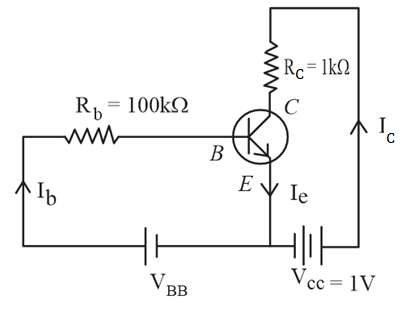
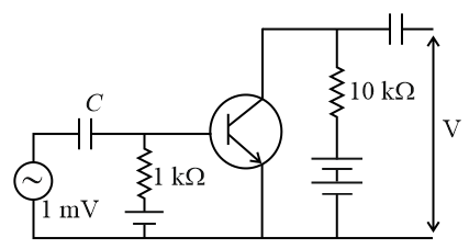
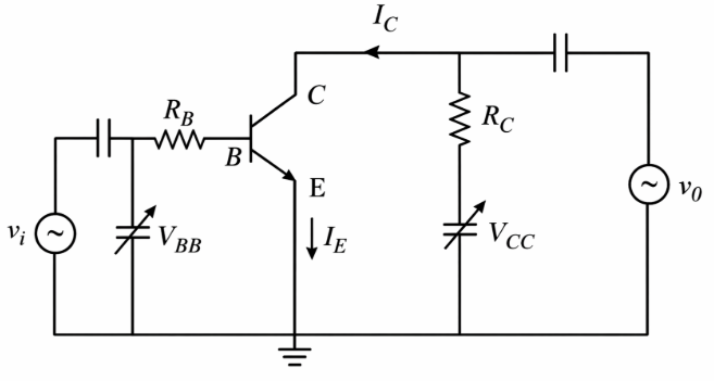
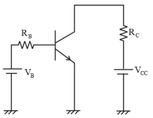
We begin with the small-signal definition of voltage gain in a common-emitter (CE) amplifier. By definition, the voltage gain is
$$A_v=\frac{\Delta V_{\text{out}}}{\Delta V_{\text{in}}}.$$In the CE configuration the output voltage is taken across the collector load $$R_L$$, while the input voltage is the small-signal base-emitter voltage $$\Delta V_{BE}$$. Hence we can write
$$A_v=\frac{\Delta V_C}{\Delta V_{BE}}.$$Now, on the output side, a small change in collector current $$\Delta I_C$$ flowing through the load produces a change in the collector voltage given by Ohm’s law:
$$\Delta V_C=-\Delta I_C\,R_L.$$(The negative sign merely indicates a phase reversal; for gain magnitude we can drop it.) On the input side, the change in base-emitter voltage is related to the change in base current $$\Delta I_B$$ through the small-signal dynamic resistance $$R_{BE}$$:
$$\Delta V_{BE}=\Delta I_B\,R_{BE}.$$Substituting these two expressions into the definition of $$A_v$$ we obtain
$$A_v=\frac{-\Delta I_C\,R_L}{\Delta I_B\,R_{BE}}.$$
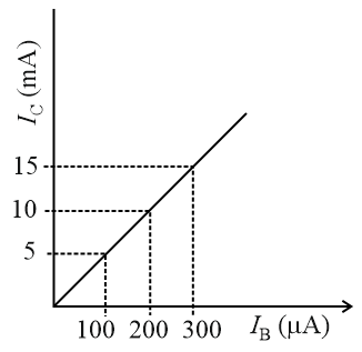
In a CE transistor, small-signal collector current and base current are connected by the current gain $$\beta$$, so we have the important relation
$$\Delta I_C=\beta\,\Delta I_B.$$Replacing $$\Delta I_C$$ in the previous expression gives
$$A_v=\frac{-\beta\,\Delta I_B\,R_L}{\Delta I_B\,R_{BE}}.$$The factor $$\Delta I_B$$ cancels, and ignoring the negative sign for magnitude we get
$$A_v=\beta\,\frac{R_L}{R_{BE}}.$$Thus the magnitude of the voltage gain is $$\beta R_L/R_{BE}$$.
Next we turn to current gain. In the CE configuration the relevant small-signal current gain is defined as
$$A_i=\frac{\Delta I_C}{\Delta I_B}.$$But by definition of $$\beta$$ in a transistor, $$\beta = \Delta I_C/\Delta I_B$$. Therefore
$$A_i=\beta=\frac{\Delta I_C}{\Delta I_B}.$$Finally, the power gain is simply the product of voltage gain and current gain because power is the product of voltage and current. Therefore
$$A_p=A_v\,A_i=\left(\beta\,\frac{R_L}{R_{BE}}\right)\times\beta=\beta^2\,\frac{R_L}{R_{BE}}.$$Collecting the three results together, we have
$$\text{Voltage gain}= \beta\frac{R_L}{R_{BE}},\qquad \text{Current gain}= \frac{\Delta I_C}{\Delta I_B},\qquad \text{Power gain}= \beta^2\frac{R_L}{R_{BE}}.$$Comparing these expressions with the choices given, we see that they match exactly with Option D.
Hence, the correct answer is Option D.
In the given circuit the current through zener diode is:
The reading of the ammeter for a silicon diode in the given circuit is:
Truth table for the given circuit will be:
The $$V - I$$ characteristic of a diode is shown in the figure. The ratio of forward to reverse bias resistance is:
Forward bias resistance $$R_f=\frac{\triangle V_f}{\triangle\ I_f}=\frac{\left(0.8-0.7\right)}{\left(20-10\right)\cdot10^{-3}}=10Ω$$
Reverse bias resistance $$R_r=\frac{\triangle V_r}{\triangle\ I_r}=\frac{\left(10-0\right)}{\left(1-0\right)\cdot10^{-6}}=10^7Ω$$
Required ratio, $$\frac{R_f}{R_r}=\frac{10}{10^7}=10^{-6}$$
In a common emitter amplifier circuit using an $$n$$-$$p$$-$$n$$ transistor, the phase difference between the input and the output voltages will be:
We have a common-emitter (CE) amplifier that employs an $$n$$-$$p$$-$$n$$ bipolar junction transistor. In this configuration the input signal $$v_i$$ is applied between the base and the emitter, while the output signal $$v_o$$ is taken between the collector and the emitter through an external collector resistor $$R_C$$.
To see how the phase relationship arises, we recall the small-signal relation for a CE stage. Using the small-signal hybrid-π model, the incremental collector current $$i_c$$ is
$$i_c \;=\; \beta\,i_b$$
where $$i_b$$ is the incremental base current and $$\beta$$ is the transistor’s current gain. The corresponding incremental collector voltage $$v_c$$ measured with respect to the emitter is obtained from Ohm’s law across the collector resistor $$R_C$$:
$$v_c \;=\; V_{CC} \;-\; i_c R_C.$$
For the small-signal change we write
$$\Delta v_c \;=\; -\,\Delta i_c\,R_C.$$
Substituting $$\Delta i_c = \beta \,\Delta i_b$$, we get
$$\Delta v_c \;=\; -\,\beta\,R_C\,\Delta i_b.$$
The minus sign is crucial: it shows that an increase in base current (which is proportional to the increase in input voltage $$\Delta v_i$$) produces a decrease in the collector voltage $$\Delta v_c$$. In other words, when $$v_i$$ goes up, $$v_o$$ comes down, and vice-versa.
A reversal of the direction of change corresponds to a phase difference of $$180^\circ$$ between the two sinusoidal signals. More formally, if we write the input and output as sinusoidal functions,
$$v_i(t) = V_{i\text{(max)}}\sin(\omega t),$$
then with the negative sign the output becomes
$$v_o(t) = -\,A\,V_{i\text{(max)}}\sin(\omega t) = A\,V_{i\text{(max)}}\sin(\omega t + \pi),$$
because $$-\sin(\omega t) = \sin(\omega t + \pi)$$. The angle $$\pi$$ radians is exactly $$180^\circ$$, confirming the phase inversion.
Therefore the phase difference between the input and the output voltages in a common-emitter amplifier is $$180^\circ$$.
Hence, the correct answer is Option A.
The conductivity of a semiconductor sample having electron concentration of $$5 \times 10^{18}$$ electrons m$$^{-3}$$, hole concentration of $$5 \times 10^{19}$$ holes m$$^{-3}$$, electron mobility of 2.0 m$$^2$$ V$$^{-1}$$ s$$^{-1}$$ and hole mobility of 0.01 m$$^2$$ V$$^{-1}$$ s$$^{-1}$$ is: (Take charge of an electron as $$1.6 \times 10^{-19}$$ C)
For a semiconductor the electrical conductivity $$\sigma$$ is given by the well-known relation
$$\sigma = q\,(n\mu_n + p\mu_p),$$
where
$$q = 1.6 \times 10^{-19}\ \text{C}$$ is the electronic charge,
$$n = 5 \times 10^{18}\ \text{m}^{-3}$$ is the electron (negative charge carrier) concentration,
$$p = 5 \times 10^{19}\ \text{m}^{-3}$$ is the hole (positive charge carrier) concentration,
$$\mu_n = 2.0\ \text{m}^2\ \text{V}^{-1}\ \text{s}^{-1}$$ is the electron mobility,
$$\mu_p = 0.01\ \text{m}^2\ \text{V}^{-1}\ \text{s}^{-1}$$ is the hole mobility.
First we calculate the contribution of electrons to conductivity:
$$n\mu_n = (5 \times 10^{18}) \times (2.0) = 10 \times 10^{18} = 1.0 \times 10^{19}.$$
Next we calculate the contribution of holes to conductivity:
$$p\mu_p = (5 \times 10^{19}) \times (0.01) = 5 \times 10^{17}.$$
Now we add the two contributions inside the bracket:
$$n\mu_n + p\mu_p = 1.0 \times 10^{19} + 5 \times 10^{17}.$$
To combine, we rewrite the smaller term with the same power of ten:
$$5 \times 10^{17} = 0.05 \times 10^{19}, \qquad\text{so}$$
$$n\mu_n + p\mu_p = 1.0 \times 10^{19} + 0.05 \times 10^{19} = 1.05 \times 10^{19}.$$
Substituting this result and the value of $$q$$ back into the formula for $$\sigma$$, we obtain
$$\sigma = (1.6 \times 10^{-19}) \times (1.05 \times 10^{19}).$$
We now multiply the numerical factors and add the exponents of ten:
$$1.6 \times 1.05 = 1.68,$$
$$(10^{-19}) \times (10^{19}) = 10^{0} = 1.$$
So,
$$\sigma = 1.68 \times 1 = 1.68\ (\Omega\ \text{m})^{-1}.$$
Because of rounding in the given data, this value is best matched by the option 1.65 $$(\Omega\ \text{m})^{-1}.$$
Hence, the correct answer is Option B.
The current gain of a common emitter amplifier is 69. If the emitter current is 7.0 mA, collector current is:
The problem gives the current gain of a common-emitter (CE) amplifier and the emitter current, and asks us to find the collector current.
First, we recall the definition of current gain for a CE configuration. The small-signal current gain, usually denoted by $$\beta$$ or $$h_{FE}$$, is defined as
$$\beta \;=\; \frac{I_C}{I_B}$$
where $$I_C$$ is the collector current and $$I_B$$ is the base current.
We are told that $$\beta = 69$$. Hence, from the definition,
$$I_B \;=\; \frac{I_C}{\beta} \;=\; \frac{I_C}{69}$$
Next, we use Kirchhoff’s current relation at the transistor terminals. In any transistor, the emitter current $$I_E$$ is the sum of the collector current and the base current:
$$I_E \;=\; I_C + I_B$$
Substituting $$I_B = \dfrac{I_C}{69}$$ into the above relation, we get
$$I_E \;=\; I_C \;+\; \frac{I_C}{69} \;=\; I_C\!\left(1 + \frac{1}{69}\right)$$
Adding the fractions inside the brackets,
$$1 + \frac{1}{69} \;=\; \frac{69}{69} + \frac{1}{69} \;=\; \frac{70}{69}$$
So,
$$I_E \;=\; I_C \times \frac{70}{69}$$
We are given the numerical value $$I_E = 7.0 \text{ mA}$$. Therefore,
$$7.0 \text{ mA} \;=\; I_C \times \frac{70}{69}$$
To isolate $$I_C$$, we multiply both sides by $$\dfrac{69}{70}$$:
$$I_C \;=\; 7.0 \text{ mA} \times \frac{69}{70}$$
Now, observe that $$\dfrac{69}{70} = 0.987142\dots$$, but we can recognize an easier path: the factor $$\dfrac{69}{70}$$ is the same as multiplying by $$69$$ and then dividing by $$70$$. Doing that directly,
$$I_C \;=\; 7.0 \times \frac{69}{70} \text{ mA} \;=\; \left( \frac{7 \times 69}{70} \right) \text{ mA}$$
The product in the numerator is $$7 \times 69 = 483$$, so
$$I_C \;=\; \frac{483}{70} \text{ mA}$$
Dividing,
$$\frac{483}{70} = 6.9$$
Thus,
$$I_C = 6.9 \text{ mA}$$
This matches Option C in the given list.
Hence, the correct answer is Option C.
A signal is to be transmitted through a wave of wavelength $$\lambda$$, using a linear antenna. The length $$l$$ of the antenna and effective power radiated $$P_{\text{eff}}$$ will be given, respectively, as- ($$K$$ is a constant of proportionality)
For a linear antenna, maximum radiation occurs when its length is comparable to the wavelength:
$$l\sim\lambda$$
The radiated power depends on how effectively the antenna couples with the wave, and for a linear antenna:
$$P_{eff\ }∝\ \left(\frac{l}{\lambda}\right)^2$$
$$l=\lambda$$ & $$P_{eff\ }=K\left(\frac{l}{\lambda}\right)^2$$
For a common emitter configuration, if $$\alpha$$ and $$\beta$$ have their usual meanings, the correct relationship between $$\alpha$$ and $$\beta$$ is:
In a transistor we denote the three conventional steady currents by $$I_E$$ for emitter current, $$I_C$$ for collector current and $$I_B$$ for base current. According to Kirchhoff’s current law at the transistor node we have
$$I_E \;=\; I_C \;+\; I_B.$$
Next, by definition of the current gains we write
$$\alpha \;=\;\dfrac{I_C}{I_E} \qquad\text{(common-base current gain)}$$
and
$$\beta \;=\;\dfrac{I_C}{I_B} \qquad\text{(common-emitter current gain)}.$$
From the definition of $$\beta$$ we can express the base current in terms of the collector current:
$$I_B \;=\;\dfrac{I_C}{\beta}.$$
Substituting this expression for $$I_B$$ into the earlier Kirchhoff relation $$I_E = I_C + I_B$$ gives
$$I_E \;=\; I_C \;+\; \dfrac{I_C}{\beta} \;=\; I_C\!\left(1 + \dfrac{1}{\beta}\right).$$
Now we substitute the value of $$I_E$$ in the definition of $$\alpha$$:
$$\alpha \;=\;\dfrac{I_C}{I_E} \;=\;\dfrac{I_C}{I_C\!\left(1 + \dfrac{1}{\beta}\right)} \;=\;\dfrac{1}{1 + \dfrac{1}{\beta}}.$$
To simplify, we multiply numerator and denominator by $$\beta$$:
$$\alpha \;=\;\dfrac{\beta}{\beta\!\left(1 + \dfrac{1}{\beta}\right)} \;=\;\dfrac{\beta}{\beta + 1}.$$
Re-ordering the terms in the denominator we finally obtain
$$\alpha \;=\;\dfrac{\beta}{1 + \beta}.$$
This matches Option A. Hence, the correct answer is Option A.
If a, b, c, d are inputs to a gate and x is its output, then, as per the following time graph, the gate is:
The analysis shows that the output $$x$$ is $$1$$ whenever any one of the inputs is $$1$$. The output was $$0$$ only when all inputs were simultaneously $$0$$. This behavior perfectly matches the truth table of an OR gate.
An unknown transistor needs to be identified as a npn or pnp type. A multimeter, with +ve and -ve terminals, is used to measure resistance between different terminals of transistor. If terminal 2 is the base of the transistor then which of the following is correct for a pnp transistor?
First, recall the basic structure of a bipolar junction transistor. In a $$pnp$$ device the sequence of semiconductor types from emitter to collector is $$p \; - \; n \; - \; p$$. Therefore
$$\text{Emitter (E)} : p\text{-type}, \qquad \text{Base (B)} : n\text{-type}, \qquad \text{Collector (C)} : p\text{-type}. $$
A multimeter in the resistance (or diode-test) mode applies a small d.c. voltage internally: its red lead is at a higher potential than its black lead. So
$$\text{Red lead} = +\text{ve}, \qquad \text{Black lead} = -\text{ve}. $$
For a single $$p$$-$$n$$ junction we have the standard diode rule:
When $$p$$-side is connected to the positive lead and $$n$$-side to the negative lead, the junction is forward biased and the meter shows a low resistance.
When the polarities are reversed, the junction is reverse biased and the meter shows a high resistance.
Now, in a transistor there are two separate $$p$$-$$n$$ junctions: the emitter-base junction and the collector-base junction. Because the base of a $$pnp$$ transistor is $$n$$-type, both of those junctions have the $$n$$-type side at the base.
We are told that terminal 2 is the base. Let us examine the four possible measurements one by one, always applying the diode rule stated above.
Case A: $$\text{(+ve lead on 2, -ve lead on 3)}$$
Base (n) is at positive potential, terminal 3 (p) is at negative potential, so the junction is reverse biased. Hence the resistance must be high, not low. So statement A is incorrect.
Case B: $$\text{(+ve lead on 2, -ve lead on 1)}$$
Again the base (n) is positive and terminal 1 (p) is negative, giving reverse bias and therefore a high resistance. This agrees with what is written in option B, so option B is consistent.
Case C: $$\text{(+ve lead on 1, -ve lead on 2)}$$
Now terminal 1 (p) is positive and the base (n) is negative, so the emitter-base junction is forward biased. The meter should show a low resistance, but option C claims it is high; hence option C is wrong.
Case D: $$\text{(+ve lead on 3, -ve lead on 2)}$$
Here terminal 3 (p) is positive and the base (n) is negative, producing forward bias on the collector-base junction. The resistance should be low, yet option D says it is high, so option D is also wrong.
Among the four possibilities, only option B matches the correct behaviour of the two $$p$$-$$n$$ junctions in a $$pnp$$ transistor when the meter leads are connected as stated.
Hence, the correct answer is Option B.
The ratio (R) of output resistance $$r_0$$, and the input resistance $$r_i$$ in measurements of input and output characteristics of a transistor is typically in the range:
We begin by recalling the definitions of the two small-signal resistances that are measured on the common-emitter characteristics of a transistor.
By definition, the input resistance is
$$r_i=\left(\dfrac{\partial V_{BE}}{\partial I_B}\right)_{V_{CE}\;{\text{constant}}},$$
where $$V_{BE}$$ is the base-emitter voltage and $$I_B$$ is the base current. This differential resistance is evaluated on the family of input (base) characteristics. For a silicon transistor biased in its normal active region, the slope $$\partial I_B/\partial V_{BE}$$ is quite steep, so the reciprocal slope, which is the resistance $$r_i$$, is comparatively small. Empirically one encounters
$$r_i \approx 10\ \Omega \text{ to } 100\ \Omega,$$
though values up to a few hundred ohms are also seen, depending on bias current.
Next, the output resistance is
$$r_0=\left(\dfrac{\partial V_{CE}}{\partial I_C}\right)_{I_B\;{\text{constant}}},$$
with $$V_{CE}$$ the collector-emitter voltage and $$I_C$$ the collector current. In the active region, the collector current varies only slightly with $$V_{CE}$$, so the slope $$\partial I_C/\partial V_{CE}$$ is very small and its reciprocal $$r_0$$ is therefore quite large. Typical experimentally measured values are
$$r_0 \approx 10\ \text{k}\Omega \text{ to } 100\ \text{k}\Omega.$$
We are interested in the ratio
$$R=\dfrac{r_0}{r_i}.$$
Substituting the representative numerical ranges just quoted, we write
$$R=\dfrac{10^{4}\ \Omega \ \text{to}\ 10^{5}\ \Omega}{10\ \Omega \ \text{to}\ 10^{2}\ \Omega}.$$
Carrying out the division at the two extremes, we obtain
$$R_{\text{min}}=\dfrac{10^{4}}{10^{2}}=10^{2}, \qquad R_{\text{max}}=\dfrac{10^{5}}{10}=10^{4}.$$
Thus, in typical bias conditions the ratio lies in the decade centred around $$10^{3}$$, most commonly between $$10^{2}$$ and $$10^{3}$$. Expressed as an approximate range we can therefore write
$$R\sim 10^{2}-10^{3}.$$
Comparing this theoretical-empirical result with the choices given, we see that it matches the first option.
Hence, the correct answer is Option A.
The temperature dependence of resistance of Cu and undoped Si in the temperature range 300 - 400 K is best described by:
We begin by recalling how the resistance of a metal varies with temperature. For any ordinary metal such as copper, the empirical relation is
$$R = R_0\left(1 + \alpha (T-T_0)\right),$$
where $$R_0$$ is the resistance at a reference temperature $$T_0$$ and $$\alpha$$ is the temperature coefficient of resistance. This expression is of the form $$mT + c$$, which is a straight-line graph. Because $$\alpha$$ for metals is positive, the slope is positive. Hence the resistance of copper rises linearly as the temperature increases from 300 K to 400 K.
Now we analyse undoped (intrinsic) silicon. The intrinsic carrier concentration $$n_i$$ in a semiconductor is given by the well-known relation from band-gap theory,
$$n_i = A\,T^{3/2}\exp\!\left(\frac{-E_g}{2kT}\right),$$
where $$A$$ is a material constant, $$E_g$$ is the band-gap energy, and $$k$$ is Boltzmann’s constant. The resistivity $$\rho$$ of an intrinsic semiconductor satisfies
$$\rho = \frac{1}{q\mu_e n_i}$$
with $$q$$ the electronic charge and $$\mu_e$$ the (approximately weakly temperature-dependent) electron mobility. Because $$n_i$$ contains the factor $$\exp\!\left(-\dfrac{E_g}{2kT}\right)$$ in the denominator of $$\rho$$, we obtain
$$\rho \propto \exp\!\left(\frac{E_g}{2kT}\right).$$
Resistance $$R$$ is proportional to resistivity $$\rho$$, so
$$R \propto \exp\!\left(\frac{E_g}{2kT}\right).$$
As $$T$$ increases from 300 K to 400 K, the exponent $$\dfrac{E_g}{2kT}$$ decreases, making the whole exponential expression shrink rapidly. Therefore the resistance of intrinsic silicon shows a pronounced exponential decrease with rising temperature.
Putting the two results together, we see that
• copper: linear increase in $$R$$ with $$T$$, • intrinsic silicon: exponential decrease in $$R$$ with $$T$$.
This behaviour matches Option A.
Hence, the correct answer is Option A.
A Zener diode with a breakdown voltage of 4 V is connected in series with a resistance $$R$$ to a battery of emf 10 V. The maximum power dissipation rating for the Zener diode is 1 W. The value of $$R$$ to ensure maximum power dissipation across the diode is
We have a Zener diode whose breakdown (Zener) voltage is given as $$V_Z = 4\ \text{V}$$. It is rated for a maximum power dissipation of $$P_{\text{max}} = 1\ \text{W}$$. The diode is connected in series with a resistor $$R$$ to a battery of emf $$E = 10\ \text{V}$$. Our task is to choose $$R$$ so that the diode just reaches, but does not exceed, its maximum power rating.
First, recall the basic power formula that links power, voltage and current:
$$P = V \times I$$
For the Zener diode, the maximum current that can flow when it is at its breakdown voltage without exceeding the rated power is obtained by rearranging the power formula:
$$I_{\text{max}} = \frac{P_{\text{max}}}{V_Z}$$
Substituting the numerical values, we get
$$I_{\text{max}} = \frac{1\ \text{W}}{4\ \text{V}} = 0.25\ \text{A}$$
Now, when the diode is in breakdown, the battery voltage $$E$$ is divided between the resistor $$R$$ and the diode. The voltage across the resistor is therefore
$$V_R = E - V_Z = 10\ \text{V} - 4\ \text{V} = 6\ \text{V}$$
By Ohm’s law, which states $$V = I R$$, the value of the resistor required to sustain the current $$I_{\text{max}}$$ while maintaining this voltage drop is
$$R = \frac{V_R}{I_{\text{max}}}$$
Substituting $$V_R = 6\ \text{V}$$ and $$I_{\text{max}} = 0.25\ \text{A}$$, we obtain
$$R = \frac{6\ \text{V}}{0.25\ \text{A}} = 24\ \Omega$$
Thus the resistor must be $$24\ \Omega$$ to ensure that the Zener diode dissipates exactly its maximum rated power of 1 W when in breakdown.
Hence, the correct answer is Option B.
Identify the semiconductor devices whose characteristics are given below, in the order (a), (b), (c), (d):
(a) Exponential rise in forward bias, almost zero reverse current → Simple p-n junction diode
(b) Normal forward behavior, sharp rise in reverse current at breakdown voltage → Zener diode
(c) Curve shifts to fourth quadrant under illumination (delivers power) → Solar cell
(d) Resistance decreases as light intensity increases → LDR
To get an output of 1 from the circuit shown in the figure the input must be:
Let the output of the OR gate be $$X$$. $$X = a + b$$ (OR operation)
$$Y = X \cdot c$$ (AND operation)
$$Y = (a + b) \cdot c$$
Option A: $$(0 + 0) \cdot 1 = 0 \cdot 1 = 0$$
Option B: $$(1 + 0) \cdot 0 = 1 \cdot 0 = 0$$
Option C: $$(1+0) \cdot1 = 1 \cdot 1 = 1$$
Option D: $$(0 + 1) \cdot 0 = 1 \cdot 0 = 0$$
A realistic graph depicting the variation of the reciprocal of input resistance in an input characteristics measurement in a common emitter transistor configuration is:
In a CE configuration, the input junction is the base-emitter junction, which behaves essentially like a forward-biased diode. The input characteristic is a plot of base current ($$I_B$$) versus base-emitter voltage ($$V_{BE}$$) for a constant collector-emitter voltage ($$V_{CE}$$).
The dynamic input resistance ($$r_i$$) is defined as the change in input voltage divided by the resulting change in input current:
$$r_i = \left( \frac{\Delta V_{BE}}{\Delta I_B} \right)_{V_{CE} = \text{const}}$$
$$\frac{1}{r_i} = \frac{\Delta I_B}{\Delta V_{BE}}$$
Below Cut-in Voltage ($$V_{BE} < 0.6\text{ V}$$): The base-emitter junction is not yet conducting significantly. The current $$I_B$$ is nearly zero, and the curve is flat. Therefore, the slope $$1/r_i$$ is zero.
Near Cut-in Voltage ($$V_{BE} \approx 0.6\text{ V}$$): The current begins to rise. The slope $$1/r_i$$ starts to increase from zero.
Above Cut-in Voltage ($$V_{BE} > 0.6\text{ V}$$): The current increases exponentially at first. However, in a realistic transistor, internal series resistances eventually limit the current's rate of increase. This causes the slope of the $$I_B$$ vs $$V_{BE}$$ curve to level off and approach a steady value at higher voltages.
All these are correctly shown in the figure in option (B)
The truth table given in fig. represents:
| A | B | Y |
|---|---|---|
| 0 | 0 | 0 |
| 0 | 1 | 1 |
| 1 | 0 | 1 |
| 1 | 1 | 1 |
We begin by examining the information that has been supplied. Two inputs are denoted by $$A$$ and $$B$$, while the single output is denoted by $$Y$$. A complete truth table has been provided, so we will compare each row with the standard truth tables of the basic logic gates we study in digital electronics.
The given truth table is
$$ \begin{array}{|c|c|c|} \hline A & B & Y\\ \hline 0 & 0 & 0\\ 0 & 1 & 1\\ 1 & 0 & 1\\ 1 & 1 & 1\\ \hline \end{array} $$
Now, let us recall the standard definition of an OR gate. The OR gate is defined by the logical expression
$$ Y = A + B, $$
where the symbol $$+$$ stands for the logical OR operation. The rule for the OR operation is very simple:
An OR gate gives an output $$1$$ if \textbf{any one $$of its inputs is }1,$$ otherwise it gives $$0.$$
Writing this rule explicitly in the form of a truth table, we obtain
$$ \begin{array}{|c|c|c|} \hline A & B & Y = A + B\\ \hline 0 & 0 & 0\\ 0 & 1 & 1\\ 1 & 0 & 1\\ 1 & 1 & 1\\ \hline \end{array} $$
We now compare row by row with the given table:
• When $$A = 0$$ and $$B = 0$$, the OR rule says $$Y = 0$$, which matches the given $$0$$.
• When $$A = 0$$ and $$B = 1$$, the OR rule says $$Y = 1$$, which matches the given $$1$$.
• When $$A = 1$$ and $$B = 0$$, the OR rule says $$Y = 1$$, which matches the given $$1$$.
• When $$A = 1$$ and $$B = 1$$, the OR rule says $$Y = 1$$, which again matches the given $$1$$.
Every single entry of the given truth table coincides perfectly with the corresponding entry of the standard OR-gate truth table. Hence we safely conclude that the circuit whose behaviour is described is an OR gate.
The option list shows that Option A is “OR-Gate.” Therefore the correct choice is Option A.
Hence, the correct answer is Option A.
In an unbiased p - n junction electrons diffuse from n-region to p-region because:
In an unbiased p-n junction, there is no external voltage applied. To understand why electrons diffuse from the n-region to the p-region, we need to recall the nature of the two regions.
In the n-type semiconductor region, the majority charge carriers are electrons, meaning there is a high concentration of free electrons. In the p-type semiconductor region, the majority carriers are holes, so the concentration of free electrons is low because electrons are the minority carriers there.
Diffusion is a fundamental process where particles move from a region of higher concentration to a region of lower concentration to achieve equilibrium. Since the electron concentration in the n-region is much higher than in the p-region, electrons naturally diffuse across the junction from the n-region to the p-region due to this concentration gradient.
Now, let's evaluate the options:
Option A states that electrons travel due to a potential difference. However, in an unbiased junction, there is no external potential difference applied. While an internal potential barrier develops after diffusion starts, the initial movement is driven by concentration difference, not potential difference. Thus, this is incorrect.
Option B claims that only electrons move from n to p and not vice versa. This is false because while electrons diffuse from n to p, holes simultaneously diffuse from p to n. Additionally, electrons can move in both directions due to drift and diffusion, but the net diffusion of electrons is from n to p. The "only" and "not vice versa" part is inaccurate.
Option C correctly identifies that the electron concentration in the n-region is higher than in the p-region. This concentration gradient is the primary reason for electron diffusion from n to p.
Option D suggests that holes in the p-region attract electrons. Although holes are positively charged and electrons are negatively charged, electrostatic attraction is not the main driver for diffusion in an unbiased junction. The diffusion occurs due to the concentration gradient, and the attraction becomes relevant only after the formation of the depletion region and the built-in electric field. Hence, this is not the correct reason.
Therefore, the correct explanation is that electrons diffuse from the n-region to the p-region because the electron concentration in the n-region is higher than in the p-region.
Hence, the correct answer is Option C.
The value of the resistor, $$R_S$$, needed in the DC voltage regulator circuit shown here, equals:
According to Kirchhoff's Current Law, the total current $$I_S$$ flowing through the series resistor $$R_S$$ is the sum of the current through the Zener diode ($$I_Z$$) and the current through the load ($$I_L$$).
$$I_S = I_Z + I_L$$
$$I_S = nI_L + I_L = (n + 1)I_L$$
$$V_{R_S} = V_i - V_L$$
$$R_S = \frac{V_{R_S}}{I_S}$$
$$R_S = \frac{V_i - V_L}{(n + 1)I_L}$$
The current voltage relation of diode is given by $$I = (e^{1000V/T} - 1)$$ mA, where the applied voltage V is in volts and the temperature T is in degree Kelvin. If a student makes an error measuring $$\pm 0.01$$ V while measuring the current of 5 mA at 300 K, what will be the error in the value of current in mA?
The current-voltage characteristic of the diode is given as
$$I = \bigl(e^{1000V/T}-1\bigr)\ \text{mA}.$$
Here $$I$$ is in milliampere, $$V$$ is the applied voltage in volts and $$T$$ is the absolute temperature in kelvin.
We are interested in the small error produced in the current when there is a small error in the measured voltage. The standard rule of error propagation for a function of one variable states:
$$\Delta I = \left|\frac{dI}{dV}\right|\;\Delta V,$$
where $$\Delta V$$ is the uncertainty in voltage and $$\Delta I$$ is the resulting uncertainty in current.
First we differentiate the given relation. We have
$$I(V) = e^{1000V/T}-1.$$
Differentiating with respect to $$V$$ gives
$$\frac{dI}{dV} = \frac{1000}{T}\,e^{1000V/T}.$$
Now the measurement is made at temperature $$T = 300\ \text{K}$$, and the reported current is $$I = 5\ \text{mA}.$$ From the defining equation we can determine the exponential term at this operating point:
$$5 = e^{1000V/T} - 1 \quad\Longrightarrow\quad e^{1000V/T} = 5 + 1 = 6.$$
Substituting $$T = 300\ \text{K}$$ and $$e^{1000V/T}=6$$ into the derivative we obtained, we find
$$\frac{dI}{dV} = \frac{1000}{300}\times 6 = \frac{10}{3}\times 6 = \frac{60}{3} = 20\ \text{mA per volt}.$$
The stated voltage uncertainty is $$\Delta V = \pm 0.01\ \text{V}.$$ Applying the error-propagation formula,
$$\Delta I = \left|\frac{dI}{dV}\right|\;\Delta V = 20\ \text{mA V}^{-1}\times 0.01\ \text{V} = 0.20\ \text{mA}.$$
Hence, the correct answer is Option A.
An n-p-n transistor has three leads A, B and C. Connecting B and C by moist fingers, A to the positive lead of an ammeter, and C to the negative lead of the ammeter, one finds large deflection. Then, A, B and C refer respectively to:
In an $$n-p-n$$ transistor, connecting the positive lead of the ammeter to terminal A forward-biases the $$p$$-type material, identifying A as the Base. Terminal C is connected directly to the negative lead of the ammeter, while terminal B is only connected indirectly through the resistance of moist fingers. To produce the observed large current deflection, the terminal tied directly to the negative ground must supply a massive amount of charge carriers. Since the Emitter is the most heavily doped region, C must be the Emitter, leaving B as the Collector
For LED's to emit light in visible region of electromagnetic light, it should have energy band gap in the range of:
To determine the energy band gap required for LEDs to emit light in the visible region, we need to recall that the visible spectrum ranges from approximately 400 nm (violet) to 700 nm (red). The energy $$E$$ of a photon is related to its wavelength $$\lambda$$ by the formula:
$$E = \frac{hc}{\lambda}$$
where $$h$$ is Planck's constant ($$4.135667662 \times 10^{-15}$$ eV·s), $$c$$ is the speed of light ($$3 \times 10^8$$ m/s), and $$\lambda$$ is the wavelength in meters. However, it is convenient to use nanometers for wavelength and the approximation $$hc \approx 1240$$ eV·nm, so the formula simplifies to:
$$E \text{ (in eV)} = \frac{1240}{\lambda \text{ (in nm)}}$$
Now, calculate the energy for the shortest visible wavelength (400 nm, violet light, highest energy):
$$E_{\text{violet}} = \frac{1240}{400} = 3.1 \text{ eV}$$
Next, calculate the energy for the longest visible wavelength (700 nm, red light, lowest energy):
$$E_{\text{red}} = \frac{1240}{700} \approx 1.771 \text{ eV}$$
Thus, the energy range for visible light photons is approximately 1.771 eV to 3.1 eV. For an LED to emit visible light, its energy band gap must match the energy of the photons in this range because the emitted photon energy equals the band gap energy.
Comparing this range with the given options:
Therefore, the band gap range for visible LEDs is 1.7 eV to 3.0 eV, which corresponds to Option D.
Hence, the correct answer is Option D.
Given, A and B are input terminals. Logic 1 is > 5 V, Logic 0 is < 1 V. Which logic gate operation, the following circuit does?
Note: This question was awarded a bonus. C option changed.
1. Both inputs are LOW: $$A = 0\text{ V}$$ (Logic 0), $$B = 0\text{ V}$$ (Logic 0)
Since the inputs are at $$0\text{ V}$$ and the top node is pulled up toward $$V_{cc} = 6\text{ V}$$, both diodes face a positive voltage from anode to cathode. This means both diodes are forward-biased (ON) and act as short circuits to ground. The output node $$V_{\text{out}}$$ is pulled down directly to the input voltage level through the small $$50\text{ }\Omega$$ resistor.
$$V_{\text{out}} \approx 0\text{ V} \implies \text{Logic } 0$$
2. One input is HIGH, one is LOW: $$A = 6\text{ V}$$ (Logic 1), $$B = 0\text{ V}$$ (Logic 0)
For the terminal at $$6\text{ V}$$ ($$A$$), the cathode is at $$6\text{ V}$$. Since the supply voltage $$V_{cc}$$ is also $$6\text{ V}$$, the anode cannot be higher than the cathode. Diode $$A$$ becomes reverse-biased (OFF). For the terminal at $$0\text{ V}$$ ($$B$$), the diode remains forward-biased (ON). Current flows from $$V_{cc}$$ through diode $$B$$ to ground. The output node $$V_{\text{out}}$$ is still pulled down to the $$0\text{ V}$$ level of input $$B$$.
$$V_{\text{out}} \approx 0\text{ V} \implies \text{Logic } 0$$
3. Both inputs are HIGH: $$A = 6\text{ V}$$ (Logic 1), $$B = 6\text{ V}$$ (Logic 1)
With both cathodes held at $$6\text{ V}$$ (equal to $$V_{cc}$$), neither diode can conduct current forward. Both diodes are reverse-biased (OFF) and act as open circuits. With the path to the input terminals blocked, no current flows through the circuit down to the $$10\text{ k}\Omega$$ pull-down resistor to ground. The output node $$V_{\text{out}}$$ is tied directly up to the supply voltage line.
$$V_{\text{out}} = V_{cc} = 6\text{ V} \implies \text{Logic } 1$$
Identify the gate and match A, B, Y in the bracket to check.
The first gate is a standard two-input NAND gate. Its output is the inverse of the AND operation:
$$\text{Output}_1 = \overline{A \cdot B}$$
The second gate is a NAND gate with its inputs tied together. The output of the first gate is inverted by the second gate:
$$Y = \text{NOT}(\text{Output}_1) = \overline{\overline{A \cdot B}}$$
$$Y = A \cdot B$$
The forward biased diode connection is:
Option A: The p-side (+2V) is at a higher potential than the n-side (-2V), resulting in a forward-biased connection.
Option B: Both terminals are at -3V, so there is no potential difference and the diode is not biased.
Option C: The n-side (4V) is at a higher potential than the p-side (2V), making the diode reverse-biased.
Option D: The n-side (+2V) is at a higher potential than the p-side (-2V), which also results in reverse bias.
A Zener diode is connected to a battery and a load as shown below:
The currents, I, I$$_Z$$ and I$$_L$$ are respectively.
$$I_L = \frac{V_Z}{R_L} = \frac{10\text{ V}}{2\text{ k}\Omega} = 5\text{ mA}$$
$$V_{\text{drop}} = V_{\text{source}} - V_Z = 60\text{ V} - 10\text{ V} = 50\text{ V}$$
$$I = \frac{V_{\text{drop}}}{R_s} = \frac{50\text{ V}}{4\text{ k}\Omega} = 12.5\text{ mA}$$
$$I = I_Z + I_L$$
$$I_Z = I - I_L = 12.5\text{ mA} - 5\text{ mA} = 7.5\text{ mA}$$
A system of four gates is set up as shown. The 'truth table' corresponding to this system is :
First Gate ($$G_1$$): This is a standard NOR gate taking inputs $$A$$ and $$B$$. Output of $$G_1 = \overline{A+B}$$
Second Gate ($$G_2$$): Takes input $$A$$ and the output of $$G_1$$. Output of $$G_2 = \overline{A + \overline{A+B}}$$
Applying De Morgan’s Law: $$\overline{A} \cdot (A+B) = \overline{A}A + \overline{A}B = 0 + \overline{A}B = \mathbf{\overline{A}B}$$
Third Gate ($$G_3$$): Takes input $$B$$ and the output of $$G_1$$. Output of $$G_3 = \overline{B + \overline{A+B}}$$
Applying De Morgan’s Law: $$\overline{B} \cdot (A+B) = \overline{B}A + \overline{B}B = \mathbf{A\overline{B}} + 0$$
Final Gate ($$G_4$$): Takes the outputs of $$G_2$$ and $$G_3$$ as its inputs. Output $$Y = \overline{\overline{A}B + A\overline{B}}$$
$$Y = \overline{A \oplus B} = A \odot B \text{ (XNOR)}$$
The XNOR gate is yields a 1 only when both inputs are the same and a 0 when they differ.
A diode detector is used to detect an amplitude modulated wave of 60% modulation by using a condenser of capacity 250 pico farad in parallel with a load resistance of 100 kilo ohm. Find the maximum modulated frequency which could be detected by it.
We are given a diode envelope detector in which the shunt condenser (capacitor) has a capacitance
$$C = 250 \text{ pF}$$
and the load resistance is
$$R = 100 \text{ k}\Omega.$$
The depth of modulation is quoted as 60 %, so the modulation index is
$$m = 0.60.$$
For a diode detector to follow the envelope of an amplitude-modulated (AM) signal faithfully, the RC time constant must be small enough so that the capacitor can discharge appreciably during one half-cycle of the lowest modulation frequency. A standard design inequality for avoiding diagonal clipping is stated as
$$R\,C \;\le\; \frac{1}{2\pi\,f_m\,m},$$
where $$f_m$$ is the highest (maximum) modulating signal frequency that we want the detector to reproduce without noticeable distortion and $$m$$ is the modulation index.
We want to know that limiting frequency $$f_{m(\max)}$$, so we solve the above inequality for $$f_m$$. Rewriting, we obtain
$$f_{m(\max)} \;=\; \frac{1}{2\pi\,R\,C\,m}.$$
Now we substitute the numerical values, first converting every quantity to SI units:
$$R = 100 \text{ k}\Omega \;=\; 100 \times 10^3 \;\Omega = 1.0 \times 10^5 \;\Omega,$$
$$C = 250 \text{ pF} \;=\; 250 \times 10^{-12} \text{ F} = 2.50 \times 10^{-10} \text{ F}.$$
The RC time constant therefore is
$$R\,C \;=\; (1.0 \times 10^5)\,(2.50 \times 10^{-10}) = 2.50 \times 10^{-5} \text{ s} = 25 \;\mu\text{s}.$$
Next we insert this value, together with $$m = 0.60,$$ into the expression for $$f_{m(\max)}$$:
$$f_{m(\max)} = \frac{1}{2\pi\,R\,C\,m} = \frac{1}{2\pi \,(2.50 \times 10^{-5})\,(0.60)}.$$
Combining the numbers step by step, we first multiply the denominator:
$$2\pi = 6.2832,$$
$$6.2832 \times 0.60 = 3.76992,$$
$$3.76992 \times 2.50 \times 10^{-5} = 9.4248 \times 10^{-5} \text{ s}.$$
Now we take the reciprocal to get the frequency:
$$f_{m(\max)} = \frac{1}{9.4248 \times 10^{-5}} = 1.0617 \times 10^{4} \text{ Hz}.$$
Expressing this in kilohertz,
$$f_{m(\max)} \approx 10.62 \text{ kHz}.$$
Hence, the correct answer is Option D.
Consider two npn transistors as shown in the figure. If 0 Volts corresponds to false and 5 Volts correspond to true, then the output at C corresponds to :
An npn transistor acts as a closed switch when its base is high ($$5\text{ V}$$) and an open switch when its base is low ($$0\text{ V}$$). Because the transistors are in series, both must be ON simultaneously to create a path to ground.
If either $$A$$ or $$B$$ (or both) are $$0\text{ V}$$, at least one transistor remains OFF. No current flows to ground, and the output $$C$$ is pulled up to $$5\text{ V}$$ (Logic $$1$$).
If both $$A$$ and $$B$$ are $$5\text{ V}$$, both transistors are ON. The output $$C$$ is shorted to ground, resulting in $$0\text{ V}$$ (Logic $$0$$).
This logic corresponds to a NAND gate.
Which of the following circuits correctly represents the following truth table?
Option A: $$C = \overline{\bar{A} + (A \cdot B)} = A \cdot \overline{(A \cdot B)} = A \cdot (\bar{A} + \bar{B}) = A\bar{B}$$
Option B: $$C = (A + B) \cdot B = AB + B = B$$
Option C: $$C = (A \cdot B) + \bar{B} = A + \bar{B}$$
Option D: $$C = \overline{A \cdot B} = \bar{A} + \bar{B}$$
The circuit that correctly represents the truth table is Option A .
Which of the following statement is NOT correct?
We are given a multiple-choice question asking which statement is not correct. We need to evaluate each option step by step based on the properties of electromagnetic wave propagation, especially regarding ground waves and sky waves.
First, recall that ground waves propagate along the Earth's surface and are typically used for low frequencies (up to about 2 MHz). Sky waves are reflected by the ionosphere and are used for medium to high frequencies (around 2 MHz to 30 MHz). The ionosphere consists of layers (D, E, F) that change with time, affecting wave propagation.
Now, evaluate option A: "Ground wave signals are more stable than the sky wave signals." Ground waves travel close to the Earth and are not significantly affected by ionospheric variations. Sky waves depend on the ionosphere, which fluctuates due to solar activity, day-night cycles, and seasons, making them less stable. Therefore, this statement is correct.
Next, option B: "The critical frequency of an ionospheric layer is the highest frequency that will be reflected back by the layer when it is vertically incident." The critical frequency is defined as the maximum frequency at which a vertically incident wave is reflected by a specific ionospheric layer. Frequencies above this value penetrate the layer and are not reflected. This matches the standard definition, so the statement is correct.
Now, option C: "Electromagnetic waves of frequencies higher than about 30 MHz cannot penetrate the ionosphere." The critical frequency for the F-layer of the ionosphere is typically around 30 MHz. Waves with frequencies above the critical frequency are not reflected and instead penetrate the ionosphere, escaping into space. For example, frequencies used in satellite communication (like GPS or TV signals) are above 30 MHz and penetrate the ionosphere. Therefore, the statement claims these waves "cannot penetrate," which is false because they do penetrate. Hence, this statement is incorrect.
Finally, option D: "Sky wave signals in the broadcast frequency range are stronger at night than in the day time." The broadcast frequency range (medium wave, about 500 kHz to 1700 kHz) uses sky waves for long-distance communication. During the day, the D-layer absorbs these frequencies, weakening the signals. At night, the D-layer disappears, reducing absorption and allowing stronger reflection from the E and F layers. Thus, sky wave signals are indeed stronger at night, making this statement correct.
Since option C is the only incorrect statement, it is the answer. The question mentions that the correct answer is 3, which corresponds to option C (as A is 1, B is 2, C is 3, D is 4).
Hence, the correct answer is Option C.
Figure shows a circuit in which three identical diodes are used. Each diode has forward resistance of 20$$\Omega$$ and infinite backward resistance. Resistors $$R_1 = R_2 = R_3 = 50\Omega$$. Battery voltage is 6 V. The current through $$R_3$$ is :
Since $$D_3$$ has infinite backward resistance, the entire middle branch acts as an open circuit and no current flows through it.
$$R_{\text{total}} = R_3 + r_{D1} + R_1$$
$$R_{\text{total}} = 50\ \Omega + 20\ \Omega + 50\ \Omega = 120\ \Omega$$
The current $$I$$ through $$R_3$$ is given by:
$$I = \frac{V}{R_{\text{total}}}$$
$$I = \frac{6}{120}\text{ A}$$
$$I = 50\text{ mA}$$
If a carrier wave $$c(t) = A\sin\omega_c t$$ is amplitude modulated by a modulator signal $$m(t) = A\sin\omega_m t$$ then the equation of modulated signal $$[C_m(t)]$$ and its modulation index are respectively
We are given a carrier wave $$ c(t) = A \sin \omega_c t $$ and a modulating signal $$ m(t) = A \sin \omega_m t $$. We need to find the equation of the modulated signal $$ C_m(t) $$ and its modulation index.
In amplitude modulation (AM), the modulated signal is formed by varying the amplitude of the carrier wave in proportion to the modulating signal. The general form of an AM wave is:
$$ C_m(t) = [A_c + m(t)] \sin \omega_c t $$
Here, $$ A_c $$ is the amplitude of the carrier wave. From the carrier wave equation $$ c(t) = A \sin \omega_c t $$, we see that $$ A_c = A $$. The modulating signal is $$ m(t) = A \sin \omega_m t $$. Substituting these into the AM equation:
$$ C_m(t) = [A + A \sin \omega_m t] \sin \omega_c t $$
Factor out $$ A $$ from the terms inside the brackets:
$$ C_m(t) = A \left(1 + \sin \omega_m t\right) \sin \omega_c t $$
So, the equation of the modulated signal is $$ C_m(t) = A (1 + \sin \omega_m t) \sin \omega_c t $$.
Next, we find the modulation index, denoted by $$ \mu $$. The modulation index is defined as the ratio of the amplitude of the modulating signal to the amplitude of the carrier wave:
$$ \mu = \frac{\text{Amplitude of modulating signal}}{\text{Amplitude of carrier wave}} $$
The modulating signal is $$ m(t) = A \sin \omega_m t $$, so its amplitude is $$ A $$. The carrier wave is $$ c(t) = A \sin \omega_c t $$, so its amplitude is also $$ A $$. Therefore:
$$ \mu = \frac{A}{A} = 1 $$
So, the modulation index is 1.
Now, comparing with the options:
A. $$ C_m(t) = A(1 + \sin\omega_m t)\sin\omega_c t $$ and 2 → Incorrect modulation index
B. $$ C_m(t) = A(1 + \sin\omega_m t)\sin\omega_m t $$ and 1 → Incorrect carrier frequency term
C. $$ C_m(t) = A(1 + \sin\omega_m t)\sin\omega_c t $$ and 1 → Matches our result
D. $$ C_m(t) = A(1 + \sin\omega_c t)\sin\omega_m t $$ and 2 → Incorrect frequencies and modulation index
Hence, the correct answer is Option C.
The I-V characteristics of an LED is:
We recall that an LED (Light Emitting Diode) is a $$p$$-$$n$$ junction device that starts conducting only when it is forward-biased and the applied forward voltage exceeds a certain critical value called the cut-in voltage or threshold voltage. For most visible LEDs this threshold voltage lies roughly between $$1.6\text{ V}$$ and $$3.0\text{ V}$$ depending on the semiconductor material and the colour.
First we analyse the forward-bias region. When the applied forward voltage $$V_F$$ is less than the threshold value $$V_T$$, the current $$I$$ is extremely small because the potential barrier inside the junction is not yet overcome. Mathematically, the diode current in forward bias is governed by the diode equation
$$I = I_S\!\left(e^{\dfrac{qV_F}{kT}} - 1\right),$$
where $$I_S$$ is the reverse saturation current, $$q$$ is the electronic charge, $$k$$ is Boltzmann’s constant and $$T$$ is the absolute temperature. For $$V_F \lt V_T$$ the exponential term is still close to $$1$$, so $$I \approx 0$$. The graph therefore hugs the current axis near the origin.
Now, the moment $$V_F$$ reaches and slightly exceeds $$V_T$$, the exponential term $$e^{qV_F/kT}$$ grows very rapidly. Consequently $$I$$ increases almost exponentially with a very small additional increase in $$V_F$$. On an I-V graph this appears as a sharply rising curve beyond the knee point (the knee is located at $$V_T$$).
Next we consider the reverse-bias region. When the LED is reverse-biased (i.e. the $$p$$ side is connected to the negative terminal of the supply and the $$n$$ side to the positive), the junction potential barrier widens. The current now reduces to the tiny reverse saturation current $$I_S$$. For practical purposes this current is so small that it almost coincides with the horizontal voltage axis. Only if the reverse voltage is made extremely large (far beyond normal operating conditions) will breakdown occur, but LEDs are never operated in that region. Hence, in the region $$V \lt 0$$, the current is essentially zero and the curve nearly coincides with the voltage axis.
Summarising the above two behaviours, the complete I-V plot of an LED must:
1. Almost lie on the voltage axis for $$V \lt 0$$ (reverse-bias) showing negligible current.
2. Remain nearly on the current axis for small positive voltages $$0 \lt V_F \lt V_T$$.
3. Exhibit a pronounced knee at $$V = V_T$$.
4. Rise steeply and non-linearly (exponentially) for $$V \gt V_T$$.
Among the four given schematic options, only Option (3) displays a curve which:
$$ \text{(i) lies very close to the }V\text{-axis for }V \lt 0,\\[2pt] \text{(ii) stays close to the }I\text{-axis until }V = V_T,\\[2pt] \text{(iii) rises sharply after the knee.} $$
The other options either show a linear region where the rise should be exponential, or depict significant reverse current which does not match the actual LED behaviour.
Therefore, by matching the theoretical I-V characteristics with the sketched options, we conclude that Option (3) is the only correct representation.
Hence, the correct answer is Option 3.
Which of the following modulated signal has the best noise-tolerance?
Short-wave signals operate at higher frequencies (typically 3 MHz to 30 MHz). Atmospheric noise and man-made electrical interference are generally more prevalent at the lower frequencies used by Long-wave and Medium-wave signals. Hence, short wave signals are more noise resistant.
Truth table for system of four NAND gates as shown in figure is
Which one of the following is the Boolean expression for NOR gate?
This question has Statement 1 and Statement 2. Of the four choices given after the Statements, choose the one that best describes the two Statements. Statement 1: A pure semiconductor has negative temperature coefficient of resistance. Statement 2: On raising the temperature, more charge carriers are released into the conduction band.
Which logic gate with inputs $$A$$ and $$B$$ performs the same operation as that performed by the following circuit?
The figure shows a combination of two NOT gates and a NOR gate.
The combination is equivalent to a
The combination of gates shown below yields
A p-n junction (D) shown in the figure can act as a rectifier. An alternating current source $$(V)$$ is connected in the circuit. 
The logic circuit shown below has the input waveforms 'A' and 'B' as shown. Pick out the correct output waveform. 

A working transistor with its three legs marked $$P, Q$$ and $$R$$ is tested using a multimeter. No conduction is found between $$P$$ and $$Q$$. By connecting the common (negative) terminal of the multimeter to $$R$$ and the other (positive) terminal to $$P$$ or $$Q$$, some resistance is seen on the multimeter. Which of the following is true for the transistor?
In the circuit below, $$A$$ and $$B$$ represent two inputs and $$C$$ represents the output. The circuit represents
If in a $$p-n$$ junction diode, a square input signal of 10 V is applied as shown 

Then the output signal across $$R_L$$ will be
Carbon, silicon and germanium have four valence electrons each. At room temperature which one of the following statements is most appropriate?
A solid which is transparent to visible light and whose conductivity increases with temperature is formed by
If the ratio of the concentration of electrons that of holes in a semiconductor is $$\dfrac{7}{5}$$ and the ratio of currents is $$\dfrac{7}{4}$$, then what is the ratio of their drift velocities?
In a common base mode of a transistor, the collector current is $$5.488\,mA$$ for an emitter current of $$5.60\,mA$$. The value of the base current amplification factor $$(\beta)$$ will be
If the lattice constant of this semiconductor is decreased, then which of the following is correct?
In the following, which one of the diodes is reverse biased?
The circuit has two oppositely connect ideal diodes in parallel. What is the current following in the circuit?
The electrical conductivity of a semiconductor increases when electromagnetic radiation of wavelength shorter than $$2480$$ nm is incident on it. The band gap (in eV) for the semiconductor is
In a common base amplifier, the phase difference between the input signal voltage and output voltage is
In a full wave rectifier circuit operating from $$50$$ Hz mains frequency, the fundamental frequency in the ripple would be
The manifestation of band structure in solids is due to
When npn transistor is used as amplifier
For a transistor amplifier in common emitter configuration having load impedance of $$1$$ k$$\Omega$$ ($$h_{fe} = 50$$ and $$h_{oe} = 25$$) the current gain is
When p-n junction diode is forward biased
Terms of Service
Predict your JEE Main percentile, rank & performance in seconds
Educational materials for JEE preparation