Sign in
Please select an account to continue using cracku.in
↓ →
Join Our JEE Preparation Group
Prep with like-minded aspirants; Get access to free daily tests and study material.
In the digital circuit shown in the figure, for the given inputs the P and Q values are :
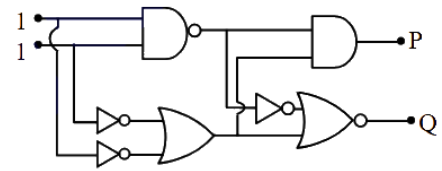
The top-left NAND gate receives inputs $$(1, 1)$$: $$\text{Output} = \overline{1 \cdot 1} = 0$$
This $$0$$ feeds directly into the top AND gate. Since any input of $$0$$ to an AND gate forces a low output, $$P$$ is immediately determined: $$P = \mathbf{0}$$
The two left NOT gates receive inputs $$(1, 1)$$, turning them into $$(0, 0)$$.
The first OR gate processes these zeros: $$\text{Output} = 0 + 0 = 0$$
This $$0$$ splits and travels to two places:
Directly to the bottom input of the final NOR gate $$\rightarrow (0)$$.
Through the middle-right NOT gate (which inverts the first NAND's $$0$$ into a $$1$$) $$\rightarrow (1)$$.
Finally, the NOR gate processes inputs $$(1, 0)$$: $$Q = \overline{1 + 0} = \overline{1} = \mathbf{0}$$
Click on the Email ☝️ to Watch the Video Solution
Create a FREE account and get:


Educational materials for JEE preparation

Ask our AI anything

AI can make mistakes. Please verify important information.
AI can make mistakes. Please verify important information.
