Sign in
Please select an account to continue using cracku.in
↓ →
Join Our JEE Preparation Group
Prep with like-minded aspirants; Get access to free daily tests and study material.
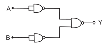
$$\text{Outputs of the first two inverter-connected NAND gates: } Y_A = \overline{A \cdot A} = \bar{A}, \quad Y_B = \overline{B \cdot B} = \bar{B}$$
$$\text{Output of the final NAND gate: } Y = \overline{Y_A \cdot Y_B} = \overline{\bar{A} \cdot \bar{B}} = \overline{\overline{A}} + \overline{\overline{B}} = A + B \implies \text{OR operation}$$
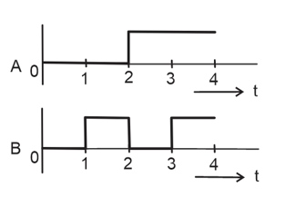
$$\text{The resulting waveform remains } 0 \text{ from } t=0 \text{ to } 1\text{, and stays at } 1 \text{ for all } t > 1$$ (As OR operation demands any one of the inputs to be $$1$$)
Click on the Email ☝️ to Watch the Video Solution
Create a FREE account and get:


Educational materials for JEE preparation

Ask our AI anything

AI can make mistakes. Please verify important information.
AI can make mistakes. Please verify important information.