Join WhatsApp Icon JEE WhatsApp Group
NCERT Solutions for Class 12 Physics

Chapter 14: Semiconductor Electronics: Materials, Devices and Simple Circuits

Download Solutions PDF
Daily JEE Updates, Tips & Important Alerts
Join 30,000+ students and stay updated with JEE notifications and preparation insights.
Join Now!
Free PDF
Complete NCERT Solution PDF for Chapter 14: Semiconductor Electronics: Materials, Devices and Simple Circuits

NCERT Solutions For Class 12 Physics Chapter 14 Semiconductor Electronics: Materials, Devices and Simple Circuits helps students understand the principles behind modern electronic devices and semiconductor technology. The page provides complete NCERT Solutions that explain concepts such as semiconductors, doping, p-n junctions, diodes, transistors, and logic gates. NCERT Solutions For Class 12 Physics make electronic concepts easier through diagrams, circuit explanations, and solved examples. The chapter connects Physics concepts with real-world applications in computers, communication systems, and electronic devices. These solutions help students revise important concepts, practise textbook questions, and prepare effectively for board examinations. Students can access the chapter PDF for quick revision and learning. The detailed explanations help learners understand semiconductor devices and their applications.
Download Solutions PDF

Examples 14.1-14.4

Example 14.1 C, Si and Ge have same lattice structure. Why is C insulator while Si and Ge intrinsic semiconductors?

Solution

Carbon, silicon and germanium all belong to Group 14 of the periodic table and each has four valence electrons that form covalent bonds in the same (diamond-type) lattice structure. The crucial difference lies in which orbit these four valence electrons occupy.

The four bonding electrons of C, Si and Ge lie in the second, third and fourth orbits respectively. As we move down the group, the valence electrons get farther from the nucleus, so they are bound less tightly. Consequently the energy required to set a valence electron free (i.e. to lift it from the valence band into the conduction band) decreases from C to Si to Ge.

This energy is precisely the energy band gap $$E_g$$ between the top of the valence band and the bottom of the conduction band. The measured values are:

$$(E_g)_\mathrm{C} \approx 5.4 \ \mathrm{eV}, \qquad (E_g)_\mathrm{Si} \approx 1.1 \ \mathrm{eV}, \qquad (E_g)_\mathrm{Ge} \approx 0.7 \ \mathrm{eV}$$

For carbon the band gap is so large ($$\approx 5.4 \ \mathrm{eV}$$) that thermal energy at room temperature ($$\approx 0.026 \ \mathrm{eV}$$) cannot lift any appreciable number of electrons into the conduction band. Hence carbon (diamond) behaves as an insulator.

For silicon and germanium the band gaps are small ($$\approx 1.1 \ \mathrm{eV}$$ and $$\approx 0.7 \ \mathrm{eV}$$). At room temperature a measurable number of electrons are thermally excited across this small gap, leaving behind holes. Both electrons and holes then contribute to conduction, so Si and Ge behave as intrinsic semiconductors.

Answer

Although C, Si and Ge have the same lattice structure, their valence electrons lie in different orbits (2nd, 3rd, 4th), so the energy band gap decreases down the group: $$(E_g)_\mathrm{C}\approx 5.4\ \mathrm{eV} > (E_g)_\mathrm{Si}\approx 1.1\ \mathrm{eV} > (E_g)_\mathrm{Ge}\approx 0.7\ \mathrm{eV}$$. The very large gap of carbon makes it an insulator, while the small gaps of Si and Ge make them intrinsic semiconductors.

Example 14.2 Suppose a pure Si crystal has $$5 \times 10^{28}$$ atoms $$\mathrm{m^{-3}}$$. It is doped by 1 ppm concentration of pentavalent As. Calculate the number of electrons and holes. Given that $$n_i = 1.5 \times 10^{16} \, \mathrm{m^{-3}}$$.

Solution

Step 1 — Number of As (dopant) atoms. The crystal is doped with arsenic at a concentration of 1 ppm (one part per million). So the number of As atoms per unit volume is one-millionth of the number of Si atoms:

$$N_\mathrm{As} = \frac{1}{10^{6}} \times 5 \times 10^{28} \ \mathrm{m^{-3}} = 5 \times 10^{22} \ \mathrm{m^{-3}}$$

Step 2 — Electron concentration. Arsenic is pentavalent. Each As atom forms four covalent bonds with neighbouring Si atoms and donates its fifth electron to the conduction band. Hence each As atom contributes one free electron, making the crystal n-type. Since the donated electrons vastly outnumber the intrinsic electrons, the electron concentration is essentially equal to the donor concentration:

$$n_e \approx N_\mathrm{As} = 5 \times 10^{22} \ \mathrm{m^{-3}}$$

Step 3 — Hole concentration. In thermal equilibrium the product of electron and hole concentrations is fixed by the law of mass action:

$$n_e \, n_h = n_i^{2}$$

Therefore

$$n_h = \frac{n_i^{2}}{n_e} = \frac{\left(1.5 \times 10^{16}\right)^{2}}{5 \times 10^{22}} \ \mathrm{m^{-3}}$$

$$n_h = \frac{2.25 \times 10^{32}}{5 \times 10^{22}} = 0.45 \times 10^{10} = 4.5 \times 10^{9} \ \mathrm{m^{-3}}$$

Since $$n_e \gg n_h$$, electrons are the majority carriers and holes are the minority carriers, confirming that the doped crystal is an n-type semiconductor.

Answer

Electron concentration $$n_e \approx 5 \times 10^{22} \ \mathrm{m^{-3}}$$ and hole concentration $$n_h = 4.5 \times 10^{9} \ \mathrm{m^{-3}}$$.

Example 14.3 Can we take one slab of p-type semiconductor and physically join it to another n-type semiconductor to get p-n junction?

Solution

No, a p-n junction cannot be formed simply by pressing a p-type slab against an n-type slab.

For a working p-n junction the p-region and the n-region must be in continuous contact, joined at the atomic scale, so that charge carriers (electrons and holes) can diffuse smoothly across the junction and form a proper depletion region with a built-in potential barrier.

When two separate slabs are simply placed together, their surfaces are never perfectly smooth — on the atomic scale they are rough and irregular. The two faces therefore touch only at a few isolated high points, and over most of the boundary there is a microscopic air gap between them. The spacing between the slabs is far larger than the inter-atomic distance in the crystal. As a result, carriers cannot diffuse across in a controlled way and no continuous crystal lattice exists across the boundary.

Hence a genuine p-n junction is not produced. In practice p-n junctions are fabricated by special techniques — for example, by diffusing a pentavalent (donor) impurity into one part of a p-type crystal, or a trivalent (acceptor) impurity into one part of an n-type crystal — so that the two regions are part of one and the same single crystal.

Answer

No. Two slabs merely pressed together touch only at isolated points with microscopic air gaps in between; the contact is not at the atomic scale, so no continuous crystal and no proper depletion layer form. A p-n junction must be made within a single crystal by controlled diffusion of impurities.

Example 14.4

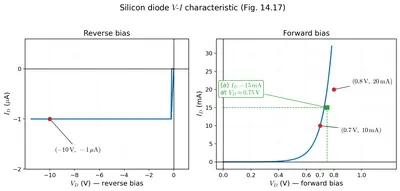
The V-I characteristic of a silicon diode is shown in the Fig. 14.17. Calculate the resistance of the diode at (a) $$I_D = 15 \, \mathrm{mA}$$ and (b) $$V_D = -10 \, \mathrm{V}$$.

(The graph shows the silicon diode characteristic with forward bias values $$I = 10 \, \mathrm{mA}$$ at $$V = 0.7 \, \mathrm{V}$$, $$I = 20 \, \mathrm{mA}$$ at $$V = 0.8 \, \mathrm{V}$$, and in reverse bias, at $$V = -10 \, \mathrm{V}$$, $$I = -1 \, \mathrm{\mu A}$$.)

Fig. 14.17
Fig. 14.17

Solution

The resistance of a diode is not constant — the V-I graph is non-linear — so we find the resistance over a small interval around the required operating point.

(a) Forward bias, around $$I_D = 15 \ \mathrm{mA}$$.

The point $$I_D = 15 \ \mathrm{mA}$$ lies between the two marked points on the forward characteristic:

$$\text{at } I = 10 \ \mathrm{mA}, \quad V = 0.7 \ \mathrm{V}$$
$$\text{at } I = 20 \ \mathrm{mA}, \quad V = 0.8 \ \mathrm{V}$$

The (dynamic) forward resistance is the ratio of the change in voltage to the change in current between these two points:

$$r_\mathrm{fb} = \frac{\Delta V}{\Delta I} = \frac{(0.8 - 0.7) \ \mathrm{V}}{(20 - 10) \ \mathrm{mA}}$$

$$r_\mathrm{fb} = \frac{0.1 \ \mathrm{V}}{10 \times 10^{-3} \ \mathrm{A}} = 10 \ \Omega$$

(b) Reverse bias, at $$V_D = -10 \ \mathrm{V}$$.

In reverse bias the current is the very small, almost constant reverse saturation current. From the graph, at $$V_D = -10 \ \mathrm{V}$$ the current is $$I_D = -1 \ \mu\mathrm{A} = -1 \times 10^{-6} \ \mathrm{A}$$.

The reverse resistance is

$$r_\mathrm{rb} = \frac{\Delta V}{\Delta I} = \frac{10 \ \mathrm{V}}{1 \times 10^{-6} \ \mathrm{A}} = 1.0 \times 10^{7} \ \Omega$$

The reverse resistance ($$10 \ \mathrm{M}\Omega$$) is enormously larger than the forward resistance ($$10 \ \Omega$$). This huge ratio is exactly why a junction diode acts as a one-way valve for current.

Answer

(a) Forward resistance $$r_\mathrm{fb} = 10 \ \Omega$$. (b) Reverse resistance $$r_\mathrm{rb} = 1.0 \times 10^{7} \ \Omega \ (= 10 \ \mathrm{M}\Omega)$$.

Exercises

14.1 In an n-type silicon, which of the following statement is true:

(a) Electrons are majority carriers and trivalent atoms are the dopants.

Solution

An n-type silicon crystal is produced by doping pure silicon with a pentavalent impurity (such as As, P or Sb). Four of the five valence electrons of each impurity atom form covalent bonds with neighbouring Si atoms, and the fifth electron is loosely bound and easily becomes a free electron.

So in n-type silicon the donated free electrons greatly outnumber the holes; electrons are the majority carriers.

This statement says electrons are majority carriers — which is correct — but it claims the dopants are trivalent. Trivalent atoms produce p-type, not n-type, material. Hence the statement is false.

Answer

False — for n-type silicon the dopants are pentavalent, not trivalent.

(b) Electrons are minority carriers and pentavalent atoms are the dopants.

Solution

In n-type silicon the pentavalent dopant donates a large number of free electrons. These electrons far outnumber the thermally generated holes, so electrons are the majority carriers and holes are the minority carriers.

This statement correctly identifies the dopants as pentavalent, but it wrongly calls electrons the minority carriers. Hence the statement is false.

Answer

False — in n-type silicon electrons are the majority carriers, not minority carriers.

(c) Holes are minority carriers and pentavalent atoms are the dopants.

Solution

n-type silicon is obtained by doping with a pentavalent impurity, which donates free electrons. The donated electrons are the majority carriers, while the few thermally generated holes are the minority carriers.

Both parts of this statement are therefore correct: holes are indeed the minority carriers, and the dopants are indeed pentavalent atoms. Hence the statement is true — this is the correct option.

Answer

True — this is the correct statement. In n-type silicon holes are the minority carriers and the dopants are pentavalent atoms.

(d) Holes are majority carriers and trivalent atoms are the dopants.

Solution

This statement describes a p-type semiconductor, not an n-type one. In n-type silicon the dopants are pentavalent (not trivalent) and the majority carriers are electrons (not holes).

Both parts of the statement are therefore wrong for n-type silicon, so the statement is false.

Answer

False — this describes p-type, not n-type, silicon. For n-type silicon the majority carriers are electrons and the dopants are pentavalent.

14.2 Which of the statements given in Exercise 14.1 is true for p-type semiconductos.

Solution

A p-type semiconductor is made by doping pure silicon (or germanium) with a trivalent impurity such as B, Al, In or Ga. Each trivalent atom has only three valence electrons, so when it bonds with four neighbouring Si atoms, one covalent bond is left incomplete — this vacancy behaves as a hole.

These holes greatly outnumber the few thermally generated electrons. Therefore, in a p-type semiconductor:

  • Holes are the majority carriers.
  • Electrons are the minority carriers.
  • The dopants are trivalent atoms.

Now compare with the four options of Exercise 14.1:

  • (a) Electrons majority, trivalent dopants — wrong (electrons are minority here).
  • (b) Electrons minority, pentavalent dopants — wrong dopant type.
  • (c) Holes minority, pentavalent dopants — describes n-type.
  • (d) Holes majority, trivalent dopants — both parts correct.

Hence statement (d) is true for a p-type semiconductor.

Answer

Statement (d) — "Holes are majority carriers and trivalent atoms are the dopants" — is true for a p-type semiconductor.

14.3 Carbon, silicon and germanium have four valence electrons each. These are characterised by valence and conduction bands separated by energy band gap respectively equal to $$(E_g)_\mathrm{C}$$, $$(E_g)_\mathrm{Si}$$ and $$(E_g)_\mathrm{Ge}$$. Which of the following statements is true?

(a) $$(E_g)_\mathrm{Si} < (E_g)_\mathrm{Ge} < (E_g)_\mathrm{C}$$

Solution

The measured band gaps of these Group-14 elements are approximately

$$(E_g)_\mathrm{C} \approx 5.4 \ \mathrm{eV}, \qquad (E_g)_\mathrm{Si} \approx 1.1 \ \mathrm{eV}, \qquad (E_g)_\mathrm{Ge} \approx 0.7 \ \mathrm{eV}$$

As we move down the group, the valence electrons occupy higher orbits and are bound less tightly, so the band gap decreases steadily: $$(E_g)_\mathrm{C} > (E_g)_\mathrm{Si} > (E_g)_\mathrm{Ge}$$.

This option claims $$(E_g)_\mathrm{Si} < (E_g)_\mathrm{Ge}$$, i.e. silicon has a smaller gap than germanium. That is wrong, since $$1.1 \ \mathrm{eV} > 0.7 \ \mathrm{eV}$$. Hence the statement is false.

Answer

False — silicon has a larger band gap than germanium, so $$(E_g)_\mathrm{Si} > (E_g)_\mathrm{Ge}$$, not smaller.

(b) $$(E_g)_\mathrm{C} < (E_g)_\mathrm{Ge} > (E_g)_\mathrm{Si}$$

Solution

Using the standard values $$(E_g)_\mathrm{C} \approx 5.4 \ \mathrm{eV}$$, $$(E_g)_\mathrm{Si} \approx 1.1 \ \mathrm{eV}$$ and $$(E_g)_\mathrm{Ge} \approx 0.7 \ \mathrm{eV}$$:

This option asserts $$(E_g)_\mathrm{C} < (E_g)_\mathrm{Ge}$$ — that carbon has a smaller gap than germanium. In fact carbon has the largest band gap of the three ($$5.4 \ \mathrm{eV} \gg 0.7 \ \mathrm{eV}$$). It also asserts $$(E_g)_\mathrm{Ge} > (E_g)_\mathrm{Si}$$, which is wrong as well.

Hence the statement is false.

Answer

False — carbon has the largest band gap, so $$(E_g)_\mathrm{C} > (E_g)_\mathrm{Ge}$$, and also $$(E_g)_\mathrm{Si} > (E_g)_\mathrm{Ge}$$.

(c) $$(E_g)_\mathrm{C} > (E_g)_\mathrm{Si} > (E_g)_\mathrm{Ge}$$

Solution

The energy band gaps of carbon, silicon and germanium are approximately

$$(E_g)_\mathrm{C} \approx 5.4 \ \mathrm{eV}, \qquad (E_g)_\mathrm{Si} \approx 1.1 \ \mathrm{eV}, \qquad (E_g)_\mathrm{Ge} \approx 0.7 \ \mathrm{eV}$$

All three elements have four valence electrons and the same lattice structure, but the valence electrons lie in successively higher orbits — the 2nd for C, the 3rd for Si and the 4th for Ge. The farther the valence electrons are from the nucleus, the more weakly they are bound, so the band gap decreases on going down the group.

This gives the ordering

$$(E_g)_\mathrm{C} > (E_g)_\mathrm{Si} > (E_g)_\mathrm{Ge}$$

which is exactly what this option states. Hence the statement is true — this is the correct option.

Answer

True — this is the correct option: $$(E_g)_\mathrm{C} > (E_g)_\mathrm{Si} > (E_g)_\mathrm{Ge}$$.

(d) $$(E_g)_\mathrm{C} = (E_g)_\mathrm{Si} = (E_g)_\mathrm{Ge}$$

Solution

This option claims all three elements have equal band gaps. They do not. Even though C, Si and Ge all have four valence electrons and the same crystal structure, their band gaps are markedly different:

$$(E_g)_\mathrm{C} \approx 5.4 \ \mathrm{eV} \neq (E_g)_\mathrm{Si} \approx 1.1 \ \mathrm{eV} \neq (E_g)_\mathrm{Ge} \approx 0.7 \ \mathrm{eV}$$

It is precisely this difference in band gaps that makes carbon an insulator while silicon and germanium are semiconductors. Hence the statement is false.

Answer

False — the band gaps are not equal; $$(E_g)_\mathrm{C} > (E_g)_\mathrm{Si} > (E_g)_\mathrm{Ge}$$.

14.4 In an unbiased p-n junction, holes diffuse from the p-region to n-region because

(a) free electrons in the n-region attract them.

Solution

Diffusion of carriers across a junction is driven by a difference in concentration, not by electrostatic attraction. Holes move from the p-side to the n-side simply because there are far more holes on the p-side — they spread out from a region of high concentration to one of low concentration, exactly as a gas diffuses.

The electrons of the n-region do not "pull" the holes across. (In fact, once the depletion layer forms, the built-in field opposes further hole diffusion.) Hence this statement is not the correct reason.

Answer

Incorrect — hole diffusion is caused by a concentration gradient, not by attraction from the n-region electrons.

(b) they move across the junction by the potential difference.

Solution

Motion of carriers caused by a potential difference (an electric field) is called drift, not diffusion. In an unbiased p-n junction the built-in potential difference across the depletion layer actually opposes the diffusion of holes from p to n — it does not cause it.

The diffusion of holes from the p-region to the n-region is caused purely by the concentration gradient. Hence this statement is not the correct reason.

Answer

Incorrect — motion due to a potential difference is drift; the barrier potential in fact opposes hole diffusion.

(c) hole concentration in p-region is more as compared to n-region.

Solution

In the p-region holes are the majority carriers, so their concentration is very high there. In the n-region holes are only the minority carriers, so their concentration is very low. This creates a large concentration gradient of holes across the junction.

Whenever there is a concentration gradient, particles diffuse from the region of higher concentration to the region of lower concentration. Therefore holes diffuse from the p-region (high hole concentration) to the n-region (low hole concentration).

This is exactly the correct reason, so this statement is true — option (c) is the correct choice.

Answer

Correct — this is the right reason. The higher hole concentration in the p-region sets up a concentration gradient that makes holes diffuse into the n-region.

(d) All the above.

Solution

Since options (a) and (b) are both incorrect explanations of hole diffusion — (a) attributes it to attraction by n-region electrons and (b) attributes it to the potential difference (which is actually drift, and in an unbiased junction opposes diffusion) — the option "All the above" cannot be correct.

Only option (c) gives the true reason. Hence statement (d) is false.

Answer

Incorrect — only statement (c) is true, so "All the above" is wrong.

14.5 When a forward bias is applied to a p-n junction, it

(a) raises the potential barrier.

Solution

Let the equilibrium (unbiased) barrier be $$V_0$$. When an external forward-bias voltage $$V_F$$ is connected with the p-side positive and the n-side negative, the external field is opposite to the junction’s internal field, so the effective barrier becomes

$$V_b = V_0 - V_F$$

Because $$V_F$$ is a positive quantity, the difference $$V_0 - V_F$$ is smaller than $$V_0$$. Hence the potential barrier is not raised; it is reduced. Therefore the statement “raises the potential barrier” is false.

Answer

False

(b) reduces the majority carrier current to zero.

Solution

Under forward bias the barrier height is lowered (see part (a)), so majority carriers can more easily diffuse across the junction. The majority-carrier current therefore increases sharply rather than dropping to zero. Hence the statement is incorrect.

Answer

False

(c) lowers the potential barrier.

Solution

Using the same reasoning as in part (a), the effective barrier under forward bias is $$V_b = V_0 - V_F$$, which is smaller than the original barrier $$V_0$$. Thus forward bias lowers the potential barrier. The statement is correct.

Answer

True

(d) None of the above.

Solution

The four alternatives offered for what a forward bias does to a p-n junction are:

  • (a) raises the potential barrier,
  • (b) reduces the majority carrier current to zero,
  • (c) lowers the potential barrier,
  • (d) none of the above.

Let the equilibrium (unbiased) barrier height be $$V_0$$. When a forward bias $$V_F$$ is applied (p-side made positive with respect to the n-side), the external field opposes the built-in field across the depletion layer, so the effective barrier becomes

$$V_b = V_0 - V_F$$

Since $$V_F$$ is positive, $$V_b$$ is smaller than $$V_0$$. That is, forward biasing lowers the potential barrier — exactly what option (c) states. The lowered barrier allows majority carriers (electrons in the n-region and holes in the p-region) to diffuse across the junction in large numbers, so the majority-carrier current actually increases sharply rather than being raised to a higher barrier (ruling out (a)) or being reduced to zero (ruling out (b)).

Since option (c) is a correct description of what forward bias does, the choice "None of the above" cannot be right. Hence statement (d) is false.

Answer

False — option (c) ("lowers the potential barrier") is correct, so "None of the above" is not the right choice.

14.6 In half-wave rectification, what is the output frequency if the input frequency is $$50 \, \mathrm{Hz}$$. What is the output frequency of a full-wave rectifier for the same input frequency.

Solution

Given data

  • Input (mains) frequency  $$f_{\text{in}} = 50\;\mathrm{Hz}$$.

Concept recall

  • In a half-wave rectifier the diode allows current during only one half of each input cycle. Therefore one output pulse appears for every complete input cycle.
  • In a full-wave rectifier (bridge or centre-tap) both halves of each input cycle are utilised. Hence two output pulses appear for every complete input cycle.

Calculations

  1. Half-wave rectifier
    The number of output cycles per second equals the number of input cycles per second, because one pulse is produced per input cycle: $$f_{\text{out (half)}} = f_{\text{in}} = 50\;\mathrm{Hz}$$
  2. Full-wave rectifier
    Now two output pulses occur during the time of one input cycle, so the output frequency is doubled: $$f_{\text{out (full)}} = 2\,f_{\text{in}} = 2 \times 50\;\mathrm{Hz} = 100\;\mathrm{Hz}$$

Result

  • Half-wave rectifier output frequency = $$50\;\mathrm{Hz}$$
  • Full-wave rectifier output frequency = $$100\;\mathrm{Hz}$$

Answer

Half-wave: $$f_{\text{out}} = 50\;\mathrm{Hz}$$
Full-wave: $$f_{\text{out}} = 100\;\mathrm{Hz}$$

NCERT Solutions for Class 12
Maths
NCERT Solutions for Class 12 Maths
Chapter-wise step-by-step
solutions with explanations
explore solutions Maths bg
Physics
NCERT Solutions for Class 12 Physics
Chapter-wise step-by-step
solutions with explanations
explore solutions Physics bg
Chemistry
NCERT Solutions for Class 12 Chemistry
Chapter-wise step-by-step
solutions with explanations
explore solutions Chemistry bg

Frequently Asked Questions

50,000+ JEE Students Trusted Our Score Calculator

Predict your JEE Main percentile, rank & performance in seconds