The plane wave propagating through the di-electric has the magnetic field component as $$H=20 e^{-ax} \cos (\omega t-0.25) a_{y} \frac{A}{m}$$ $$ (a_{x},a_{y},a_{z}$$, are the unit vectors along x, y and z axis respectively ) Determine the Polarization of the wave
ISRO Scientist or Engineer Electronics 2020
For the following questions answer them individually
In Free space, $$H=0.1 cos(\omega t-\beta x) a_{z} \frac{A}{m}$$ ($$a_{x}, a_{y}, a_{z}$$ ,are the unit vectors along x, y and z axis respectively ) The Total power passing through a square plate of side)10 cm on plane $$x + 2y = 1.0$$, is approximately :
Consider the rectangular cavity as shown below :
If $$a = c > b$$, The Dominant mode of resonance corresponding to the above Rectangular cavity is
A video camera generates data at a rate of 5 Mbps. The data is channel coded at rate $$\frac{1}{3}$$ and 8 PSK modulated. Which of the following statements is correct?
Evaluate $$\int_{-\infty}^{\infty} x^{4} f(x) dx$$, where $$f(x)=\frac{1}{\sqrt{2 \pi}}e^{-\left(\frac{x^{2}}{2}\right)}, x \in(-\infty,\infty)$$
Consider a transformation $$T:R^{3} \rightarrow R^{2}$$ where $$R^{3}$$ and $$R^{2}$$ represent three and two dimensional real column vectors respectively. Also, T(x) = Ax for some matrix A and for each x in $$R^{3}$$ How many rows and colums does A have and what is its maximum possible rank?
The output of a three element co-linear antenna array operating in a free space environment is combined after appropriate phase shifting) to maximize the signal received from a particular direction as shown in figure
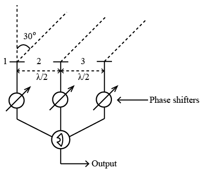
If the inter-element spacing is half of the signal wavelength and the direction of maximum response is $$30^\circ$$ from line perpendicular to the array ,what are the phases to be apllied to the each element? Consider the first element as the reference?
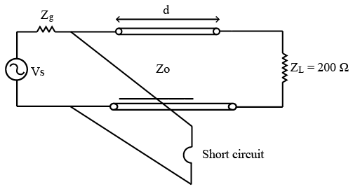
The transmission line of charecteristic impedance 50 Ω and feeding a purely resistive load of 200 Ω uses single quarter wavelength long short circuit stub which is placed at a distance d from the load .The VSWR on the transmission line section of length d and VSWR on the stub respectively are
The plane Y =O carries a uniform current density of -20 k $$\frac{mA}{m}$$ The magnetic field intensity at X =1,Y =10 and Z = —2 is
A Charge of 2 Coulombs is placed near a grounded conducting plate at a distance of m. The force acting between the charge of 2 C and ground conducting plate in Newton is
A data sequence x[n] = {1,2,3,4,5} passes through a linear time-invariant system with impulse response h[n] = {5, 4, 3, 2, 1}. The output of the filter will be
Consider a signal $$\mu (t)$$ with the fourier transform V(f).If v'(f) represents the Fourier transform of $$\mu(2t)$$, what is the relation of V'(f) and v(f)?
If one of the code words of a Hamming (7,4) code is 00010111,which of the folllowing can not be the valid code wordin the same group ?
Which of the following digital modulations can be decoded non-coherently?
A mobile antenna receives two copies of the signal transmitted by the base section .The first copy is the line of sight component and the other is a reflected component
which is 20 dB weaker in terms of power than the Los component and delayed by 100 ns .If the signal is sufficiently wide band , causing constructive and destructive interference at different frequency points with in the signal bandwidth .what will be the ratio of maximum to minimum signal level varaition across bandwidth and what will be the frequency separation between two consective maxima or minima?
An antenna with an efficiency of 90% has a maximum Radiation intensity of 0.5 W/Steradiam. Calculate the directive gain of the antenna when the input power to the antenna is 0.4 W
In a semiconductor device, if Fermi level $$(E_{F})$$ is positioned at conductive band $$(E_{c})$$. Determine the Approximate probability of finding electrons in states at $$(E_{c} + kT)$$
(where K is Boltzmann constant and T is device temperature in Kelvin)
For the following energy band diagram, determine the approximate resistivity for x > L portion of semiconductor.$$E_{g} = 1.12 eV, T=300 K, \mu_{n} = 600 cm^2/V-sec, \mu_{P} = 400 cm^2/V-sec, n_{i} = 10^{10}/cm^3$$

The radiation intensity of a given anteena is $$U = 2 (\sin \theta \sin \phi)$$ in the range $$0 \leq \theta \leq \pi$$ and $$0 \leq \phi \leq \pi$$ and 0 else where .The directivity is
Which of the following is an example of oversampling ADC architecture?
A radarreceiver has a detection SNR threshold of 10 dB for a 4 MHz bandwidthsignal at 300 MHzfrequency.If the transmit EIRP of the radar is 40 dBW andreceive $$\frac{G}{T}$$ is 10 $$\frac{dB}{K}$$, what is the minimum RadarCross Section (in dB-meter square) detectable at 10 km range? (Given : 10 log $$(4\pi)$$ = 11, 10 log(k) = -228.6, k is Boltzmannconstant).
A source generates four messages m1, m2, m3 and m4,with probabilities 0.5, 0.25, 0.125 respectively.The messages are generated independently of each other.A source coder assigns binary code to each message. Which of the following code has minimum average length and is also uniquely decodable (sequnece as per m1, m2, m3, m4)?
For the given circuit, switch remains closed for a long time and opens at t = 0 seconds. Assuming ideal model for every device find steady state magnitude of voltage at capacitor.

For the given circuit, Aspect ratio of $$M_{1}$$, transistor is $$\frac{20}{0.5}, I_{D_{1}} = 200 \mu A, V_{THO} = 0.6 V, 2 \phi_f = 0.81 V, \gamma = 0.4 V^{2}$$ and $$\mu_{n} C_{ox} = 59.5 \mu A/V^2$$. If $$V_{in} = 1.2 V$$, find the minimum value of aspect ratio of $$M_{2}$$ transistor to ramin saturated $$(\sqrt{10} = 3.16)$$

Two coherent microwave power sources of same frequency f, each generating P Watts of average power ,are combined using a four port network in the following manner

If the S-parameter of the 4-port network are $$\begin{bmatrix}0 & \frac{j}{\sqrt{2}}& \frac{-1}{\sqrt{2}}&0 \\\frac{j}{\sqrt{2}} & 0 & 0 &\frac{-1}{\sqrt{2}}\\\frac{-1}{\sqrt{2}} & 0& 0& \frac{j}{\sqrt{2}}\\0& \frac{-1}{\sqrt{2}}& \frac{j}{\sqrt{2}}&0\end{bmatrix}$$ what should be the phase difference between the inputs to maximize the output at port 2 and what is maximum the power?
Which of the following statement is wrong?
Which of the following statementis correct?
Which one plot gives the closest resemblanceto the stability factor $$S(I_{co})$$ of emitter bias configiuration of BJT with respect to $$\frac{R_{E}}{R_{B}}$$? ($$R_{E}$$ is the emitter resistance and $$R_{B}$$ is the base resistance)
For the given Amplifier Circuit find the input cutoff frequency. FET parameters are $$g_{m} = 4 mA/V, C_{gs} = 4 pf, r_{ds} = 40 K Ω, C_{gd} = 2pF$$

Which of the following digital devices requires an external refresh circuit?
What would be the maximum operating frequency of Mod-8 counter constructed With JK flip flops, having propagation delay of 8ns?
The following state diagram represents which of the input equation. (Given: $$D_{A} = [A, x, y])$$ (Where $$D_{y}$$, denotes a $$DFF$$ with output A. The x and y are the inputs to the circuit)

Which of the following logic circuits do not have no-change condition?
In VHDL following statement 18 written within a Process, where Clock frequency is 24 MHZ
If (Clock event and clock = ‘1’) then
counter_4 bit < = counter_4 bit + x "1" ;
End if;
The frequency of counter_4 bit (2) will be:
Initial voltage on $$C_{1}$$ capacitor is 3 V in the given circuit. Correct sketch of $$V_{x}$$ as a function of time is .(Threshold voltage $$(V_{th}) = 0.5 V)$$

AnSRAMhasaddresslines from $$A_{0}$$, to $$A_{19}$$ and data width from $$D_{0} to D_{15}$$. Total capacity of the SRAM will be
Which of the following digital integrated circuit cannot eebe used as wired logic connections?
The logic function implemented by following circuit can be represented as

The value of C required for sinusoidal oscillation of Frequency = 2 kHz in the given circuit is

In the given circuit, $$V_{be} = 0.7 V, V_{z} = 5.3 V, \beta = 100 . V_{o}$$ is

A 18 $$\mu F$$ - Capacitor holding of Q coulomb is connected to the circuit at time t = 0 sec.

The time at which the capacitor will be discharged to. approximately $$\frac{Q}{2.72}$$ coulombs.
Determine the value of voltage $$V_{1}$$ in the figure shown below

The Value of Voltage $$V_{1}$$, in volts is
Output characteristics of a BJT amplifier is given, Find the minimum collector current required for $$r_0$$=50 K Ω ($$r_0$$ is the output resistance)

In the given circuit, $$S_{1}$$, switch remains closed and $$S_{2}$$ remains open for the long time .At $$t = 0, S_{1}$$ opens and $$S_{2}$$ closes and remain in this position for the long time. Find drain current for $$t < 0$$ and $$t >> 0$$ respectively if, $$\mu_n C_{ox} = 100 \mu A/V^2$$ and the Aspect ratio = 2

In the circuit shown below, switch $$S_{1}$$ is closed and t = 0 seconds. Switch $$S_{2}$$, is opened at t = 0 seconds.

The current flowing through the inductor of 0:3 H at t=8 mili seconds is
The Transmission Parameters of the network given below is represented in the matrix form as $$[T]=\begin{bmatrix}A & B \\C & D \end{bmatrix}$$

Calculate the Transmission Parameter B of [T] matrix,
In the circuit shown, diodes are ideal. Which is the correct representation of transfer characteristics of the circuit?

Consider the R-L-C network shown below

The average power absorbed by the Inductor in Watts is
The total number of possible trees corresponding to the network shown below is

For an n-type Ge specimen, width = 4 mm, length = 1 mm, current (along the length of nen) = 1 mA, magnetic field (perpendicularto the current flow direction) = 0.1 $$\frac{Wb}{m^{2}}$$ and Hall voltage magnitude = 0.005 V. Calculate the majority carriers density.
The following table gives the forward characteristics of a Si diode. Estimate the temperature of a diode junction.
(Given : $$\ln (0.2) = -1.609$$)

An n-channel MOS transistor is made on a p-type substrate with Na = $$10^{15} cm^{-3}$$ Find approximate depletion charge per unit area $$(Q_{d})$$ at strong inversion.
$$\left\{\ln(10)=2.3,\sqrt{0.046} \approx 0.215, n_{i}=10^{10} cm^{-3}\right\}$$
For a p-channel Si JFET, $$N_{a} = 3 \times 10^{16} cm^{-3}, N_{d}=10^{18} cm^{-3}$$. Channel thickness dimension is $$a = 0.33 \mu m$$. Find the approximate pinch-off voltage $$V_{p}. \left\{ n_{i}=10^{10} cm^{-3}, V_{r} = 26 mV, \ln (3) = 1.098 \right\}$$
Consider the circuit shown below

The power factor of the above circuit as seen by the source is
All the Three inductors are perfectly coupled as shown below,the value of total in (in Henry) across the terminal AB is

For a uniformly doped npn transistor, find the approximate emitter injection efficiency.
Given that:
$$N_{E}=2 \times 10^{18} cm^{-3}$$, $$N_{B}=10^{17} cm^{-3}, $$N_{C}=4 \times 10^{19} cm^{-3}, $$D_{E}=8 \frac{cm^{2}}{s}$$,$$D_{c}=28 \frac{cm^{2}}{s}$$, $$D_{B}=20 \frac{cm^{2}}{s}$$,$$ x_{E}=0.5 \mu m$$, $$x_{B}=0.3 \mu m$$
In a long p-type Si-bar with cross-sectional area = 0.5 $$cm^{2}$$ and $$ N_{a}.= 2 \times 10^{17} cm^{-3}$$ extra holes $$10^{16} cm^{-3}$$ are injected Assume $$\mu_{p}=500 \frac{cm^{2}}{Vs}$$, $$n_{i}=10^{10} cm^{-3}$$ and $$ \tau_{p}= 10^{-10}s $$find minority carrier lifetime.
In a p-type Si at 300 K and $$N_a = 8 \times 10^{15} cm^{-3}$$, variation of space-charge density in the semiconductor as a function of surface potential is plotted, then select the true statement for weak inversion region. Given that $$p_{s}$$ and $$n_{s}$$ are hole and electron concentrations at the surface.
In order to ensure that the output voltage of an opamp zero, is when both its inputs are grounded
Consider the resistive network shown below, the value of Norton current across the terminal AB

The Transfer characteristic of the different types of MOSFETs is shown below , where $$I_{D}$$ is drain current and $$V_{GS}$$ is the Gate source volatge , the correct combination of MOSFET w.r.t to transfer characteristics is

Accept impurity concentartion of si at 300 K is $$10^{19} cm^{-3}$$ Calculate the concentration of donor impurity atoms that should be added so that Si is n type and the Fermi Energy is 26 meV below the conduction band edge (Given: Effective density state $$N_{c} = 2.7 \times 10^{19} cm^{-3}$$ and Thermal Volatage $$(V_{T})$$ at 300 K is 26 mv)
The electric field between twoparallel plates placed in vacuum is ‘E’. If a slab of dielectric constant $$\sqrt{3}$$ is inserted in between the plates such that the normal to the boundary makes an angle $$45^\circ$$ with the lines of electric force in between the plates. Find the angle $$(\theta)$$ between the electric lines in the medium between the plates (vacuum) and dielectrié slab.
Two parallel perfectly conducting planes of infinite extent are placed ‘b’ distance apart so that the cut-off frequency of the lowest order TE mode is 15 GHz. If additionally, two perfectly conducting planes are placed 10 mm_apart so as to form a rectangular wave guide as shown in figure. Find out the cutoff frequency of $$TE_{11}$$ mode.

Consider the AND logic circuit in which $$V_{2} = 3 V$$ and $$V_{1}$$ lies between 0 to 5 volts The output Voltage is $$V_{o}$$ .The cut-in Voltage of the Diode $$D_{1}$$ and $$D_{2}$$ is 0.6 Volts. The output voltage $$V_{o}$$ versus $$V_{1}$$ corresponding to the below network is

Following are the applications of a Buck and Boost Converters respectively
A. Regulated DC powersupplies
B. Regenerative braking of DC motors~
C .DC motor speed control.
In a MOSFET $$SiO_{2}$$, breaks down at electric field of the order of $$5 \times 10^{6} V/cm$$. For a gate oxide of thickness 1000 A and channel thickness of $$2 \mu m$$, what is the maximum $$V_{GS}$$ it can with stand ?
Which of the followingis false for a Thyristor?
A. Thyristor is a majority-carrier device
B. The forward-bias portion of Thyristors i-v characteristics has two stable operating regions.
C.The forward-bias portion of Thyristors i-v characteristics has one stable operating regions.
D. The negative gate current turns off the Thyristor.
The Zener regulator circuit shown below consists of si based Zener diode and Ge diode . The cut-in Voltage of Ge diode is 0.2 volts where cut in voltage of si-diode is 0.7 Volts.

The output Voltage $$( V_{o})$$ of the Zener Regulator Circuit is
The asymptotic bode plot for the gain magnitude of a minimum phase System G(s) is shown in figure below

The steady state error for ramp input is
Identify the Converter topologies from the figures given below:

Consider two control systems with following transfer function,
System 1 : $$G(s)=\frac{1}{3s + 1}$$
System 2 : $$G(s)=\frac{1}{s + 1}$$
Which of the following is true:
A systems open loop transfer function is given by $$G(s) = \frac{K}{s(s+2)(s+4)}$$. If the system is having a unity negative feedback which of the following is true for such system is stable ?
The Third peak overshoot and second undershootof the step response of the second order under damped system is given by
Consider the Nyquist plot of the second order underdamped system shown in the below figure

The Resonant Frequency corresponding to the Nyquist plot is
The unit step responseof a system with the transfer function $$G(s)=\frac{1-s}{1+s}$$ s given by which of the following? (A unit step function is represented by u(t))
The system $$\frac{1600}{s(s+1)(s+16)}$$ is to be compensated such that its gain-crossover frequency becomes same as its uncompensated Phase-crossover frequency. Which of the following is the phase crossover frequency of the compensated system?
A discrete-time, linear time invariant system with input sequence $$x_{n}$$, and output sequence $$Y_{n}$$ is characterised by
$$y_{n}=0.1x_{n}+0.9 y_{n-1}$$
If two such systems are connected in series, which of the following is the governing difference equation of the overall system?
The total number of feedbackloops of the signal flow graph is where R is input and C is output.

From the below given Nyquist plot,calculate the number open loop poles on the Right hand side of s-plane for the closed loop system to be Stable.


