Electron mobility of the following intrinsic elements in descending order is:
ISRO Scientist or Engineer Electronics 2015
For the following questions answer them individually
A sample of Si is doped with $$10^{17}$$ donor atoms/cm$$^3$$. Considering electron mobility in the doped Si 700 cm$$^2$$/V-sec, the approximate resistivity of the doped Si is:
Common-base current gain of a p-n-p bipolar transistor is 0.99. The common emitter current gain of the transistor is:
The electrical conductivity of a semiconductor increases when a radiation of wavelength shorter than 1000 nm is incident on it. The band gap of the semiconductor is:
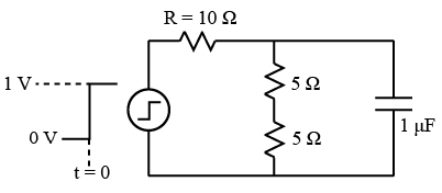
The voltage across the resistor R is:
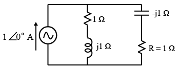
The effective resistance faced by the voltage source is:
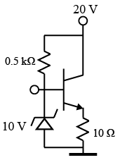
Common emitter DC current gain of the transistor is 100. The current through the 10 V Zener diode (assuming Vzs of the transistor is 0.7 V) is:
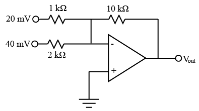
The circuit is with an ideal operational amplifier with $$\pm 10 V$$ supply. The output voltage is:
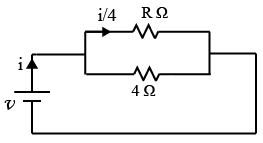
A step voltage of 10 V applied to the circuit at t = 0. The current through the resistor R just after t = 0 and at steady state are:
Which of the following addressing mode is not usable in XCH instruction of 8051 microcontroller?
In a binary source, Os occur three times:as often as 1s. What is the information contained in the 1s?
Spectrum of a signal x(t), sampled at period T, is given by:
A bandpass signal occupies the bandwidth 390 KHz to 410 KHz. What minimum sampling frequency would you use from the options giveri below, so as to avoid aliasing?
A 12-bit ADC has input signal range of $$\pm 1 V$$. The signal to quantization noise ratio if a sine wave signal with 0.25 V peak voltage is given as input is:
Identify the modulation schemes for the shown signal constellation diagram

Which of the following modulation scheme requires minimum powerfor transmission?
Which of the following channel coding scheme helpsin correcting burst errors?
A 70 MHz carrier is QPSK modulated by a 1.544 Mbps T1 data stream. The transmitter employs a raised-cosine filter with $$\alpha = 0.2$$ What is the transmitted bandwidth of the
signal?
If two tones $$f_1$$, and $$f_2$$, are amplified by a non-linear amplifier, which frequency components would be present in output?
A phaselock loop with a first order loop filter can track:
The noise figure of a device is 2. If input SNR is 37 dB, what would be output SNR?
What is the limit of Eb/No, below which reliable communication is not possible?
A satellite communication link has uplink C/No of 50 dB-Hz and downlink C/No of 47 dB-Hz. What would be overall link C/No?
A signal transmitted from an Earth station bounces back from a geostationary satellite, with an altitude of 35864 km from the Earth surface. The range from the Earth station is
38200 km. The round trip time is about: (excluding processing delays and assuming $$c = 3 \times 10^8 m/s$$)
1 mW in dBm is:
Which of the following is not true?
The following Finite State Machine (FSM) is used to detect a particular pattern in input data stream. Whenever the pattern is matched at input, output is set to ‘l’ or else output is cleared to ‘0’. For which of the following data stream, output goes to ‘1’ twice?

A digital signal processing system is described by the expression:
$$y(n) = 2x(n) + x(n - 1) + 2y(n - 1)$$
The system is:
The rectangular window hasrelative side-lobe level:
Consider the discrete time signal $$x(n) = \left\{1, 1, 1, 1, 0.5, 0.5 \right\}. y(n) = conv (\delta(n - 1), x(n))$$ is:
Consider a sequence x(n) = [2, 4, 6, 8, 0, 1, 3, 5, 7, 9]. Down-sample the sequence by 3 and then up-sample by 2. The resulting sequence is:
Power consumed in a CMOScircuit operating at frequency fis proportional to:
The phase velocity of a plane wave given by $$E_x = E_o \cos(\omega t - \beta z)$$ with a frequency of 5.0 GHz and a wavelength in the material medium of 3.0 cm is:
If the reflected wave at the load of a transmission line is 20dB below the incident wave, the SWR atthe load is:
The highest frequency for which a circular coaxial transmission line having outer diameter = 3.1 mm and inner diameter = 1.3 mm can be operated in pure TEM mode (assuming free space medium between the two conductors) should be less than:
In a communication system at 300 MHz, the receiving antenna gain is 8 dBi, the transmitting antenna gain is 10 dBi and the transmitting power level is 25 watts, the distance between the transmitter and the receiver is 1 km, the power received at the receiving antenna port (assuming the propagation medium is loss-less):
A rectangular waveguide with air medium has dimensions a = 22.86 mm and b = 10.6 mm is fed by 3 GHz carrier from a coaxial cable, which of the following is false statement for $$TE_{01}$$ mode?
$$TM_{01}$$ mode in rectangular perfect metallic waveguide is:
The directivity of a prime-focal parabolic reflector antenna is 30 dBi.If the efficiency of the antenna is 50%, the gain of the antenna is:
Ratio of skin depths of an Electromagnetic wave inside the conductor for the corresponding frequencies at 4 GHz and 9 GHz, considering the same material properties for both the frequencies is:
A Cassegrain reflector antenna has a sub-reflector whose geometrical shape is:
The beam-width and the directivity of an antenna are:
A lossless transmission line with characteristic impedance $$Z_0 = 50$$ ohm is 30 m long and operates at 2 MHz. Theline is shorted at the load, if the phase velocity = 0.6 times the velocity of light, the input impedance of the line is:
Two microwave sub-systems having respective return loss of 10 dB and 20 dB are cascaded together, the return loss at the input of the integrated system is:
A parabolic reflector antenna used for reception of data is 1 meter in diameter and operates at 30 GHz. The far field distance of this antenna for a quadratic phase error of 22.5 degree is:
A potential field is given by $$\phi = 2 xy^2 - 3 y^2z$$. If $$\hat{x}, \hat{y}, \hat{z}$$ are the unit vectors along x, y and z directions respectively, the field intensity at (0, 1, 0) is:
The VSWR of a microwaveunit is 1.5, the return loss is:
In two wire transmission line, two consecutive voltage minima are found at 20.6 caaee 25.6 cm. The operating frequency is:
A TEM mode transmission line is having distributed circuit parameters as R = 1 ohm/m, L = 200 nH/m, G = 300 $$\mu$$S/m, C = 60 pF, the line is:
A plane wave $$E = 100 \sin(\omega t - 10 x) V/m$$ in a loss less medium with $$\mu = 4 \mu_o, ε = ε_o$$ strikes another medium with 90 degree angle of incidence having $$\mu = 9 \mu_o, ε = ε_o$$, the reflection co-efficient is:
What is the functionality of following digital circuit? A is input data, CLK is system clock and Y is output.

A lossless transmission line has the distributed circuit parameters of inductance and capacitance per meter as 625 nH/m and 64 pF/m respectively, the phase constant of the line at 100 MHz is:
In the circuit if $$C1 = 2 \mu F$$ and $$C1 = 3 \mu F$$, the equipment capacitance between points A and B is:

If n number of MOSFETs with identical W/L are connected in series, then equivalent W/L is given by:
Which resource of FPGA implements combinational logic functionality?
What will be the content of Accumulator, Register-B and Overflow Flag (OV) after execution of following 8051 micro-controller assembly code?
MOV A, #65h
MOV OFOh, #14h
DIV AB
DIV AB
Average value of the waveform is:

Gain and NF of a single stage amplifier is 10 dB and 3 dB respectively. When two such amplifiers cascaded then gain and NF of cascaded amplifier will be:
Which Type of memory has constrain of minimum operating clock frequency?
Main function of helix structure in a Travelling Wave Tube (TWT) is
Equivalent circuit of FET is shown in the figure below,
where $$r_s = 100 Ω, C_{gs} = 0.1 pF$$ and $$g_m = 0.1 mho$$. For load resistance $$r_L = 500 Ω$$, the voltage gain at 1 GHz is:

Which of the following is true for an NMOS transistor operating in linear region?
Magnitude of input impedance of a $$\frac{\lambda}{8}$$ lossless 50 Ω transmission line terminated with 25 Ω is:

Pipelining techniqueis used in microprocessor to improve which of the following parameter?
In case of an ideal Class-F microwave power amplifier, time domain voltage and current waveform of the device have:
Reason for superior high frequency performance of metal-semiconductor diode compared to p-n junction diode is:
Which of the following diodes is most suitable for detection of microwave signal?
Which device is suitable for higher order RF frequency multiplier?
Input reflection coefficient ‘S11’ of the 2-port network for 50 Ω system is:

The graph below shows operating load line and I-V characteristic of a Schottky diode at two different RF power levels. Under this bias condition RF resistance of the diode:

A BJT is having common emitter current gain 100. Considering 10 V supply and $$V_{BE} = 0.7 V$$ what will be the value of $$R_C$$ and $$R_B$$ to set the quiescent point at $$I_c = 10 mA$$ and $$V_{CE} = 8 V$$

Which statement is false about microstrip line over stripline?
A high gain MESFET packaged device of case-to-channel thermal resistance of the device is $$4.5^\circ C$$/Watt provides 8 W RF output power taking 20 W DC power. What will be the channel temperature of the device if the case temperature of the device maintained at $$55^\circ C$$?
For a class-A FET power amplifier with 10 V drain supply and 2 A drain current bias providing RF load current of 1 A amplitude. What is the DC to RF efficiency for load resistance of 5 Ω?
DC to RF efficiency of an ideal class-F amplifier is:
A unilateral transistor has an output impedance $$Z_{out} = (10 - j10)Ω$$. Value of the series and shunt components of the matching network for complex conjugate match at the output of the device to 50 Ω load are:

Acommunication channel is having a bandwidth of 3000 Hz. The transmitted poweris such that the received Signal-to-Noise ratio is 1023. The maximum data rate that can be transmitted t error-free through the channel is:
A CDMA system requires $$E_b/I_o$$, of 10 dB. Each of the transmitters in the network transmits data at the rate of 1 Kbps with a PN chip rate of 1 Mbps. The maximum number of such users that the network can support is:
Laplace transform of $$e^{\theta t} \sin(\omega t)$$ is:
Under steady state condition, the energy stored in the circuit is:


