Sign in
Please select an account to continue using cracku.in
↓ →
Join Our JEE Preparation Group
Prep with like-minded aspirants; Get access to free daily tests and study material.
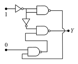
Let the output of the top NAND gate be $$Y_1$$, the middle NAND gate be $$Y_2$$, and the bottom NAND gate be $$Y_3$$.
The output stage $$Y$$ is a shared node tied directly to both upper outputs: $$Y = Y_1 = Y_2$$
Output of the first NOT gate with input 1: $$\text{Input to top NAND gate} = \overline{1} = 0$$
Since both inputs of the top NAND gate are tied to this node: $$Y_1 = \overline{0 \cdot 0} = 1 \implies Y = 1$$
Output of the second NOT gate connected below it: $$\text{Upper input to middle NAND gate} = \overline{0} = 1$$
Evaluating the bottom NAND gate with one fixed input at 0: $$Y_3 = \overline{0 \cdot Y} = \overline{0} = 1$$
Evaluating the middle NAND gate using its determined inputs: $$Y_2 = \overline{1 \cdot Y_3} = \overline{1 \cdot 1} = 0$$
Since the wire mesh forces a conflict where $$Y_1 = 1$$ and $$Y_2 = 0$$ attempt to drive the same node $$Y$$:
$$Y = Y_1 \cdot Y_2 = 1 \cdot 0 = 0$$
Create a FREE account and get:


Educational materials for JEE preparation

Ask our AI anything

AI can make mistakes. Please verify important information.
AI can make mistakes. Please verify important information.