Sign in
Please select an account to continue using cracku.in
↓ →
Join Our JEE Preparation Group
Prep with like-minded aspirants; Get access to free daily tests and study material.
For the given circuit (shown in part (A)) the time dependent input voltage $$v_{in}(t)$$ and corresponding output $$v_o(t)$$ are shown in part (B) and part (C), respectively. Identify the components that are used in the circuit between points X and Y.
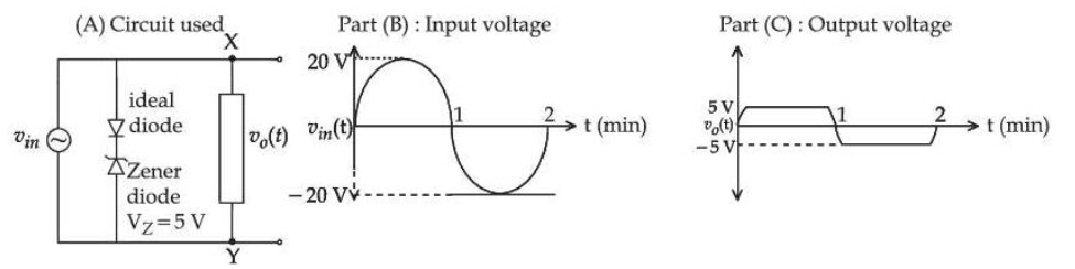
The input waveform shown in part (B) is an undistorted sinusoid that swings symmetrically above and below the 0-V axis.
The output waveform shown in part (C) is identical to the positive half-cycles of the input, whereas the entire negative half-cycles are missing (the output remains at 0 V whenever the input is negative).
This behaviour is the signature of an ideal half-wave rectifier:
• During the positive half-cycle, the rectifying element is forward-biased, it conducts, and $$v_{o}(t) \approx v_{in}(t)$$ (neglecting the small forward drop).
• During the negative half-cycle, the rectifying element is reverse-biased, it blocks, and the load sees no current, so $$v_{o}(t)=0$$.
The simplest circuit that realises a half-wave rectifier between the points X (input node) and Y (output node) is a single p-n diode (anode at X, cathode at Y) feeding a load resistor connected from Y to ground. No other passive component can reproduce exactly this “positive-half-only” transfer characteristic.
Hence the network between X and Y must consist of a forward-biased diode in series with the load, i.e. the arrangement given in Option A.
Option A which is: a single diode (anode at X, cathode at Y) forming a half-wave rectifier.
Create a FREE account and get:


Educational materials for JEE preparation

Ask our AI anything

AI can make mistakes. Please verify important information.
AI can make mistakes. Please verify important information.
