Sign in
Please select an account to continue using cracku.in
↓ →
Join Our JEE Preparation Group
Prep with like-minded aspirants; Get access to free daily tests and study material.
If $$V_A$$ and $$V_B$$ are the input voltages (either 5 V or 0 V) and $$V_0$$ is the output voltage then the two gates represented in the following circuits A and B are:
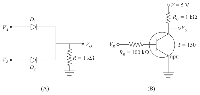
$$\text{For Circuit (A): Analysis of the diode configuration}$$
$$\text{If } V_A = 0\text{ V and } V_B = 0\text{ V: Both } D_1 \text{ and } D_2 \text{ are reverse-biased (off) } \implies V_0 = 0\text{ V}$$
$$\text{If } V_A = 5\text{ V or } V_B = 5\text{ V: At least one diode conducts (on), pulling up the output node } \implies V_0 = 5\text{ V}$$
$$\text{This truth table (0,0}\rightarrow\text{0; 0,1}\rightarrow\text{1; 1,0}\rightarrow\text{1; 1,1}\rightarrow\text{1) corresponds exactly to an OR gate.}$$
$$\text{For Circuit (B): Analysis of the common-emitter BJT configuration}$$
$$\text{If } V_B = 0\text{ V: The base-emitter junction is cut off } \implies I_C = 0 \implies V_0 = V_{CC} - I_C R_C = 5 - 0 = 5\text{ V}$$
$$\text{If } V_B = 5\text{ V: Base current drives the transistor heavily into saturation } \implies V_0 = V_{CE(\text{sat})} \approx 0\text{ V}$$
$$\text{This inversion logic (0}\rightarrow\text{1 and 1}\rightarrow\text{0) corresponds exactly to a NOT gate.}$$
Create a FREE account and get:


Educational materials for JEE preparation

Ask our AI anything

AI can make mistakes. Please verify important information.
AI can make mistakes. Please verify important information.
