Sign in
Please select an account to continue using cracku.in
↓ →
Join Our JEE Preparation Group
Prep with like-minded aspirants; Get access to free daily tests and study material.
In the following circuit, the correct relation between output ($$Y$$) and inputs $$A$$ and $$B$$ will be
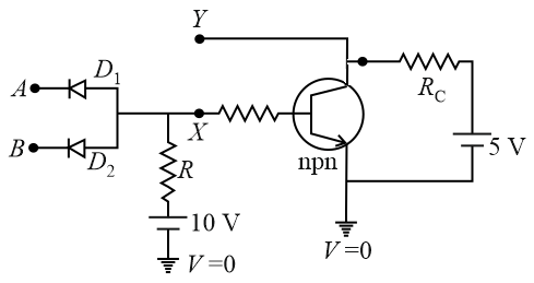
To determine the logic operation of the given circuit, we analyze the behavior of the diodes and the NPN transistor for different input combinations:
The first part of the circuit (diodes $$D_1$$ and $$D_2$$ connected to a $$-10\text{ V}$$ source through resistor R) acts as an AND gate logic for the point X:
The NPN transistor acts as a NOT gate (inverter):
| Input A | Input B | Point X (A ⋅ B) | Output Y (X) |
| 0 | 0 | 0 | 1 |
| 1 | 0 | 0 | 1 |
| 0 | 1 | 0 | 1 |
| 1 | 1 | 1 | 0 |
The output Y is the inverse of the AND operation of the inputs. This corresponds to a NAND gate.
Correct Relation:
$$\boxed{Y = \overline{AB}}$$
Correct Option: (C)
Create a FREE account and get:


Educational materials for JEE preparation

Ask our AI anything

AI can make mistakes. Please verify important information.
AI can make mistakes. Please verify important information.
